IBM unveils the industry's first 7nm chips

Scorpus

Posts: 2,162   +239
Staff member

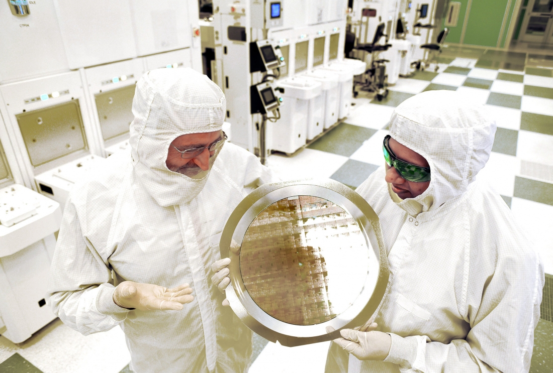
IBM, in partnership with GlobalFoundries, Samsung, and the State University of New York (SUNY), have been able to produce the world's first 7nm chips through the use of new materials and new manufacturing techniques.

For starters, IBM's 7nm chips use a FinFET transistor design that differs from existing FinFETs in that the transistor's channel is made from silicon-germanium alloy, rather than plain silicon. This is due to the fact that silicon by itself has issues with electron mobility below 10nm, which restricts current flow and hampers performance. Adding germanium to the mix has been found to resolve these issues.

These 7nm chips were produced using extreme ultraviolet (EUV) lithography, which etches features using a base wavelength of 13.5nm, significantly smaller than argon fluoride (ArF) lasers that, at 193nm, are used for current 14nm lithography. Although EUV lithography has proven to be difficult to deploy in the commercial space, it's a much better option than ArF for producing sub-10nm chips without the need for as complex optic systems.

IBM has managed to pack transistors incredibly tightly on their 7nm chips, achieving a transistor pitch of just 30nm. This leads to surface area reduction of around 50 percent compared to bleeding-edge 10nm chips, which IBM believes can result in performance and power improvements of "at least" 50 percent.

There are still some difficulties to overcome before 7nm chips can be mass produced, which is why the technology is not expected to arrive until 2017 or 2018. However, if IBM can use their research at 7nm to develop a commercially viable manufacturing process, they might just be able to beat traditional process node leader Intel, who are currently working on mass production at 10nm, to market.

Permalink to story.

 
Not only would this be a great advancement... it would actually mean competition on the silicon level, which hasn't really existed for years... and can someone ban that katieperry account... I'm not going to be earning any extra money...
 
7nm, dang that's micoscopic. Cant wait to see it in our next generation smartphones of tomorrow. Super-computer in the palm of our h.....in our pockets.
 
Honestly, it's time to start rethinking the entire architecture of chips when we get to this size.

If it were possible to produce "layered" chips where some connections only need to travel up/down a few microns instead of across the span of an entire chip, you could significantly speed up the chip without having to reduce the transistor size to impossible scales.

"Layered" chips do have the problem that you can't cool them by crushing a heatsink over the unit, but it would produce less heat naturally by using less electricity, and could possibly lead to the first "liquid cooled" die.
A little late to the dance.... This is almost a year and a half old dude....
 
Can produce 7nm state of the art silicon chips. Still can't make employee attire that doesn't look like something from a budget constrained Star Trek episode
 
Back