Surprise! iFixit has torn down the latest iPad Pro 9.7 and discovered a bunch of iPad hardware inside the well-crafted metal chassis. In fact Apple has managed to cram an enormous amount of hardware into a very small space, perhaps making it the most densely-packed iPad yet.
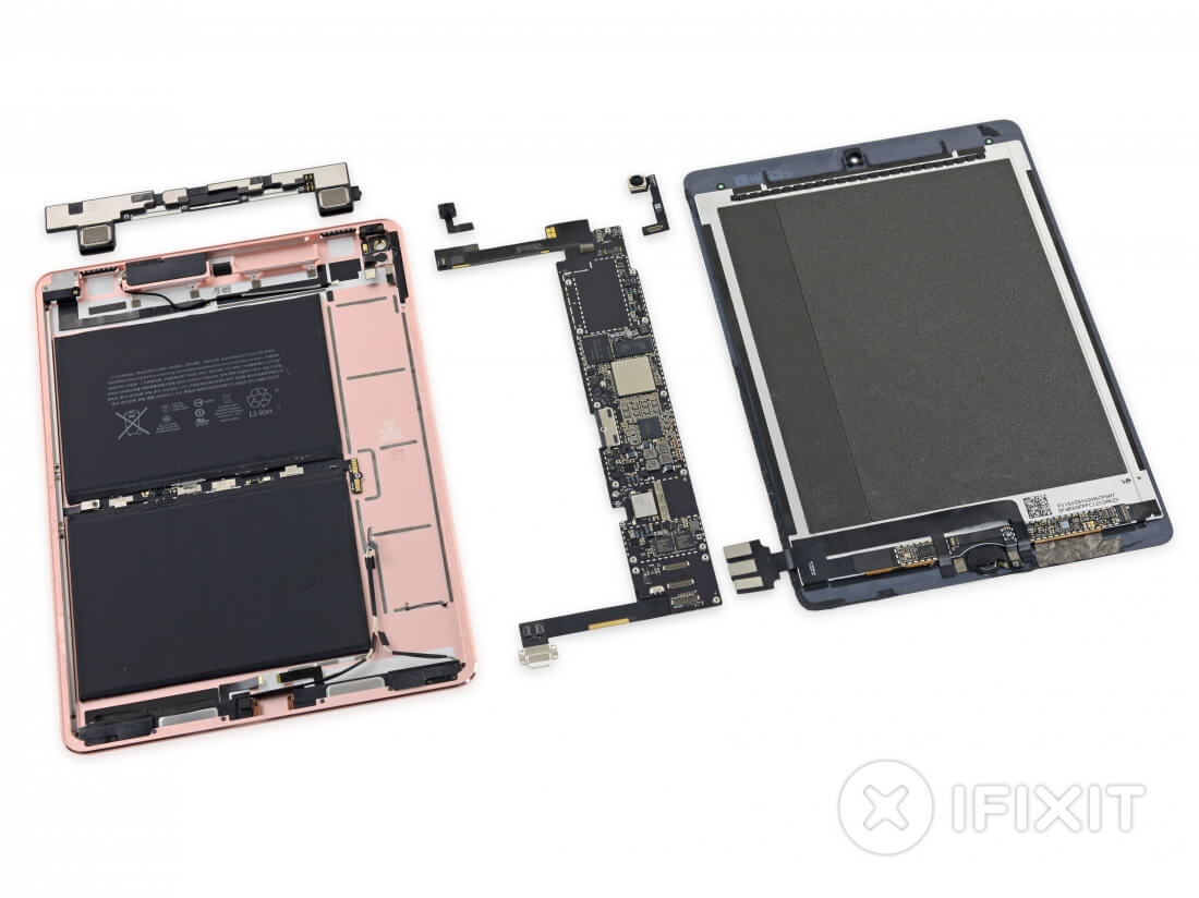
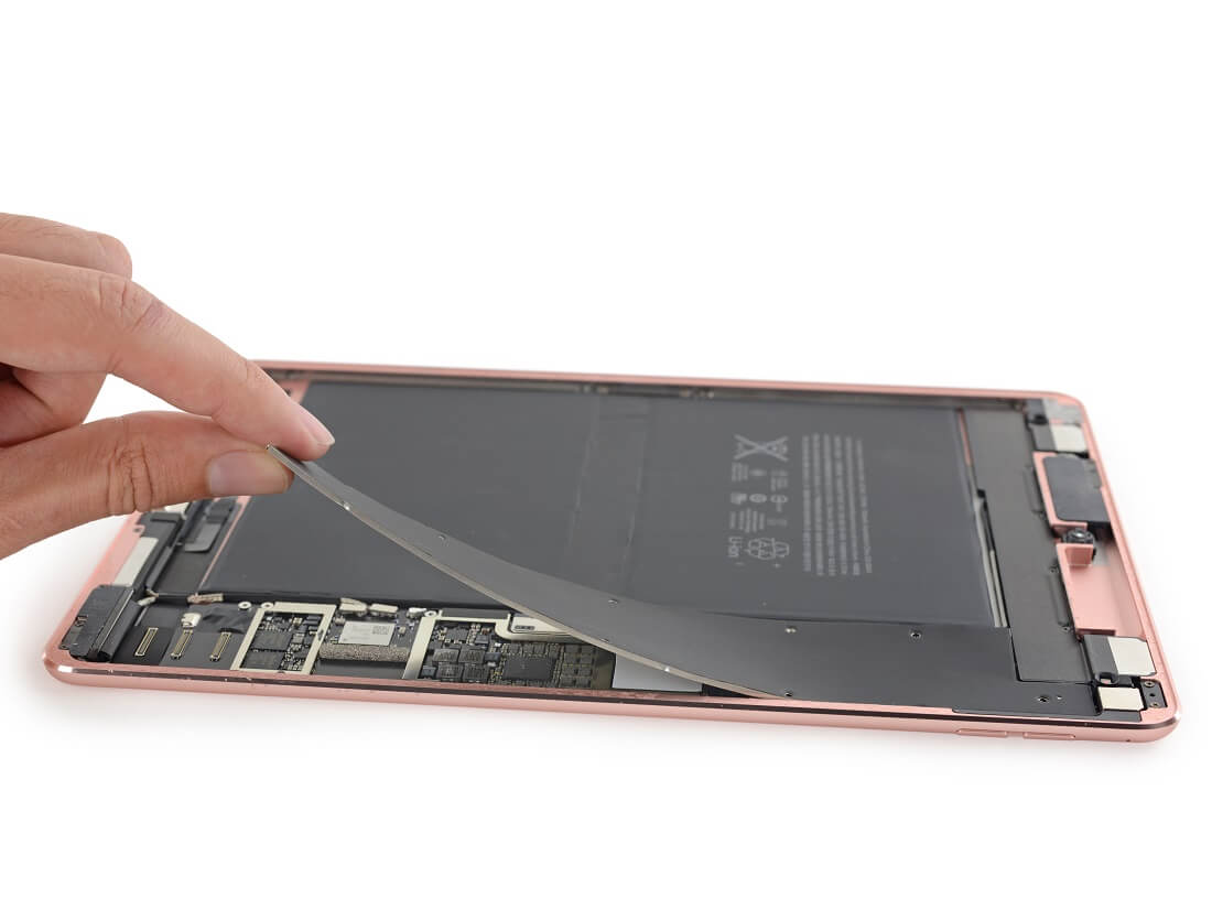
Opening up the iPad Pro 9.7 is a pretty typical process: heating, prying, and suctioning. Once the 9.7-inch 'True Tone' display is separated from the components, a massive, slim battery is exposed that occupies the vast majority of ths device's footprint. Markings on the battery indicate it has a rated capacity of 27.91 Wh, which is marginally larger than the 27.62 Wh battery in the iPad Air 2.
The logic board spans an entire side of the new iPad Pro, and it contains a collection of important chips. Almost in the middle of the board is Apple's A9X SoC, with 2 GB of Samsung LPDDR4 memory and 32 GB (in this model) of SK Hynix NAND nearby. There's also an Apple-designed Wi-Fi chip, NXP Touch ID and NFC controllers, and an array of sensors.
iFixit uncovered the four-speaker array that finally gives the 9.7-inch iPad stereo audio, as well as the 12-megapixel optically stabilized camera that's identical to the one found in the iPhone 6s.
Overall the iPad Pro 9.7-inch still scores poorly on iFixit's repairability scale, sitting at just two out of ten. This is mostly due to lots of glue used in its construction, a fused front panel that requires care when opening, and a Smart Connector port that's "virtually impossible to replace".
https://www.techspot.com/news/64321-ipad-pro-97-teardown-reveals-bunch-ipad-internals.html
