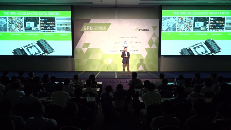
Nvidia's next-generation graphics core, codenamed 'Pascal', is expected to launch in the first half of 2016, bringing a large jump in performance that should impress the PC gaming enthusiasts out there. But before the GPU could be publicly detailed by Nvidia, a slide from the company's GTC Taiwan 2015 presentation has leaked, giving us an early look at the design of the chip.
While we aren't getting a complete look at a board featuring Nvidia's Pascal GPU, the image from GTC Taiwan 2015 does show the die closely flanked by HBM 2.0. This second-generation high bandwidth memory technology is expected to give Pascal memory bandwidth in the 1 TB/s range, double that of the HBM 1.0 AMD used with their current-gen Fiji GPUs.
Rumor has it that Nvidia will include a whopping 16 GB of HBM 2.0 with their top-end Pascal products, while the chip itself will feature up to 17 billion transistors. Nvidia will be able to cram that many transistors into a reasonable die size thanks to the use of TSMC's 16nm FinFET+ manufacturing process, which is an effective die shrink compared to current 28nm technology.

Pascal is expected to support mixed floating point precision as well, going beyond what Kepler and Maxwell support by adding FP16 execution alongside FP32 and FP64. Pascal can allegedly perform FP16 calculations at twice the rate of FP32, so if games are willing to sacrifice precision, Pascal can provide a speed boost.
When Pascal launches in the first half of 2016, it will go head to head with AMD's upcoming Arctic Islands line, which is also expected to use HBM 2.0 and be built on a 16nm process. 2016 is shaping up to be an exciting year for graphics card launches, where we might finally see significant performance gains over the previous generation.
Images courtesty of WCCFTech
