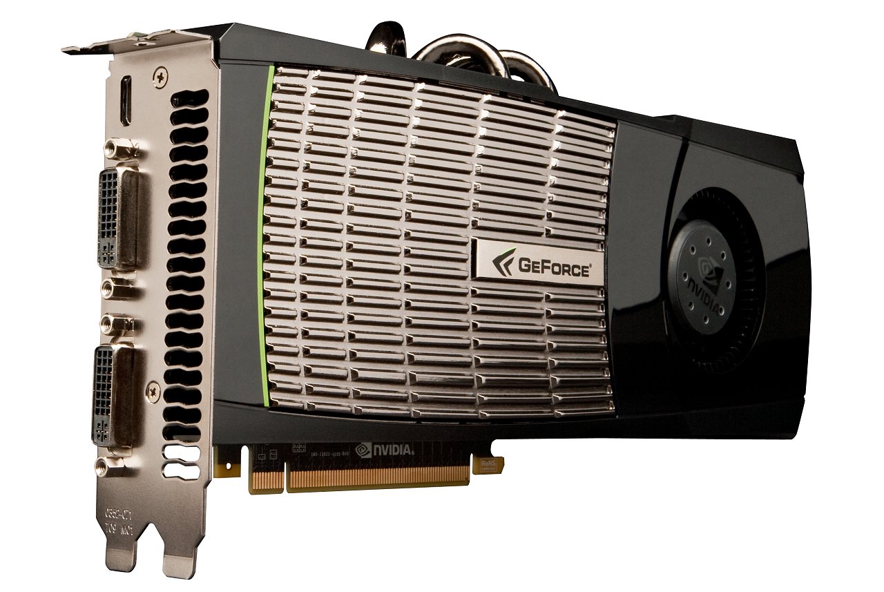
An Overview of the Fermi Architecture
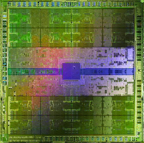
The first Fermi-based GPUs will feature some three billion transistors supporting up to 480 CUDA cores. CUDA is the hardware and software architecture that enables NVIDIA GPUs to execute programs written with C, C++, Fortran, OpenCL, DirectCompute, and other languages.
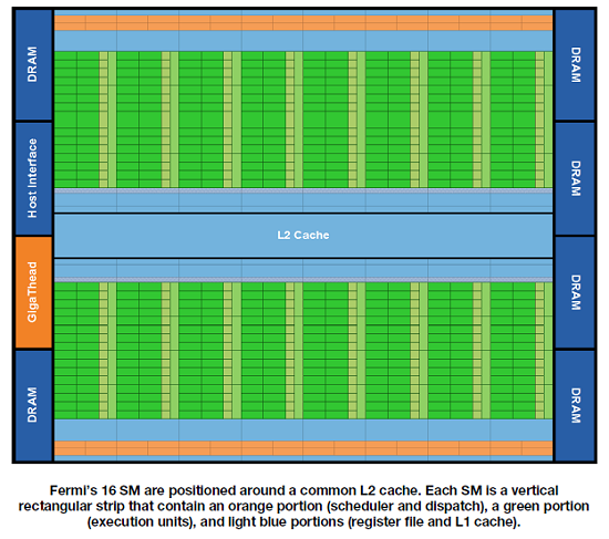
Initially the first GeForce GTX 400 series graphics cards were meant to feature 512 cores, though once again due to TMSC's poor 40nm yields the design has been scaled back. Apparently, yields are still currently lower than 50%.
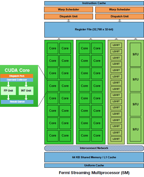
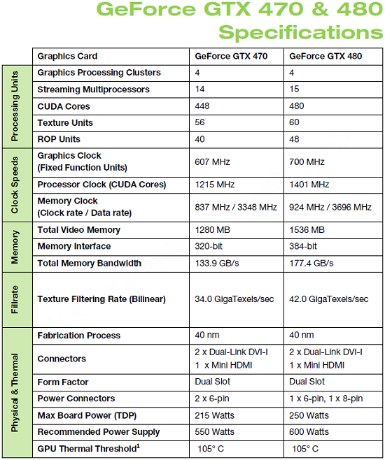
A CUDA core executes a floating point or integer instruction per clock for a thread. The 480 CUDA cores are organized in 15 Streaming Multiprocessors of 32 cores each, which is a fourfold increase over prior SM designs.
The GeForce GTX 480, for example, features 15 SMs of 32 cores for a total of 480. The GeForce GTX 470 on the other hand features 14 SMs for 448 cores. The GTX 480 has six 64-bit memory partitions for a 384-bit memory interface, supporting up to a total of 6GB of GDDR5 memory, while the GTX 470 features five 64-bit memory partitions for a 320-bit memory interface.
The Fermi architecture features a third generation streaming multiprocessor which Nvidia says introduces several architectural innovations that make it not only the most powerful SM yet built, but also the most programmable and efficient. Each CUDA processor has a fully pipelined integer arithmetic logic unit (ALU) and floating point unit (FPU), whereas previous GPUs used IEEE 754-1985 floating point arithmetic instead.
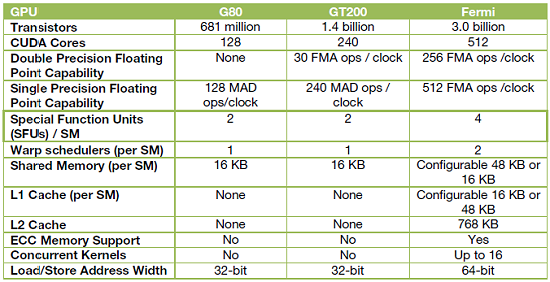
The GT200 architecture used by GeForce GTX 200 series graphics cards limited the integer ALU to 24-bit precision for multiple operations, and as a result multi-instruction emulation sequences were required for integer arithmetic. Fermi on the other hand features a newly designed integer ALU that supports full 32-bit precision for all instructions, consistent with standard programming language requirements.
One of the key architectural innovations that greatly improved both the programmability and performance of GPU applications is on-chip shared memory. Shared memory enables threads within the same thread block to cooperate, facilitates extensive reuse of on-chip data, and greatly reduces off-chip traffic. This is a key enabler for many high-performance CUDA applications.
G80 and GT200 both have 16KB of shared memory per SM. With Fermi, each SM has 64KB of on-chip memory that can be configured as 48KB of shared memory with 16KB of L1 cache, or as 16KB of shared memory with 48KB of L1 cache.
For existing applications that make extensive use of shared memory, tripling the amount of shared memory yields significant performance improvements, especially for problems that are bandwidth constrained. Applications that use shared memory as software managed cache can streamline code to take advantage of the hardware caching system, while still having access to at least 16KB of shared memory for explicit thread cooperation.
Additionally applications that don't use shared memory automatically benefit from the L1 cache, allowing high performance CUDA programs to be built with minimum time and effort. The Fermi architecture clearly has a number of impressive design aspects and features. Another that we are going to look at in more detail is called Nvidia 3D Vision Surround.
