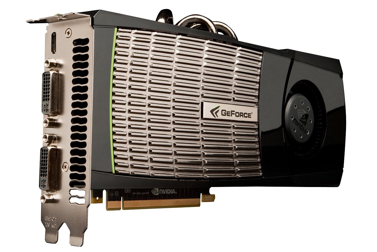
Nvidia GeForce GTX 480 in Detail
The GeForce GTX 480 was designed for maximum gaming performance. With an MSRP of $499 its intensions are quite clear. At this price point the card is anywhere from $70 to $100 more expensive than the Radeon HD 5870, and as much as $200 cheaper than the dual-GPU Radeon HD 5970.
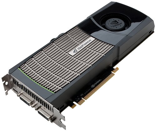
Based on the Fermi third-generation Streaming Multiprocessor (SM) architecture, the GeForce GTX 480 boasts 480 CUDA cores, which is twice the shader power of the GT200 architecture used by the GeForce GTX 280/285.
Not only has the number of cores doubled, but so have the number of ROP (Raster Operations) units with 48 in total. 8x MSAA performance has been optimized through enhanced ROP compression and texture units are also said to have been redesigned for improved efficiency and better real-world performance. In total, there are 60 of them.
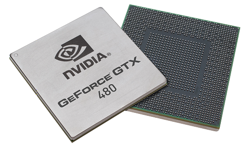
So to break it down, the GeForce GTX 480 features 4 Graphic Processing Clusters, 15 Streaming Multiprocessors, 480 CUDA Cores, 60 Texture Units and 48 Raster Operations Units. The graphics clock speed for fixed function units is 700MHz, while the CUDA Cores operate at a more aggressive 1401MHz.
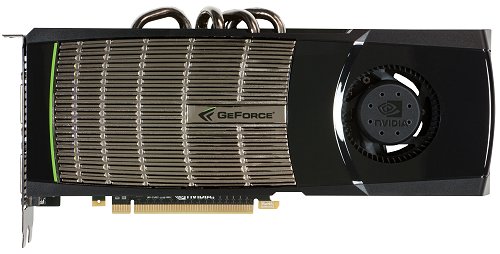
The GeForce GTX 480 is teamed with 1536MB of GDDR5 memory clocked at 924MHz (3696MHz DDR). Combine that with a memory interface of 384-bit and the end result is a peak theoretical bandwidth of 177.4GB/s or 15% more bandwidth than the Radeon HD 5870 and 12% more than the GeForce GTX 285.
All this horsepower adds up for a Thermal Design Power (TDP) of a staggering 250 watts, which is 33% greater than that of the Radeon HD 5870 and 23% greater than the GeForce GTX 285. Perhaps the most amazing thing about these figures is that the TDP of the GeForce GTX 480 is just 15% lower than that of the mighty Radeon HD 5970.
Other than the PCI Express slot, the GeForce GTX 480 draws in power though a pair of external PCI Express power connectors. The GTX 480 requires a 6-pin and an 8-pin connector and Nvidia recommends using at least a 600 watt power supply when using this card.
