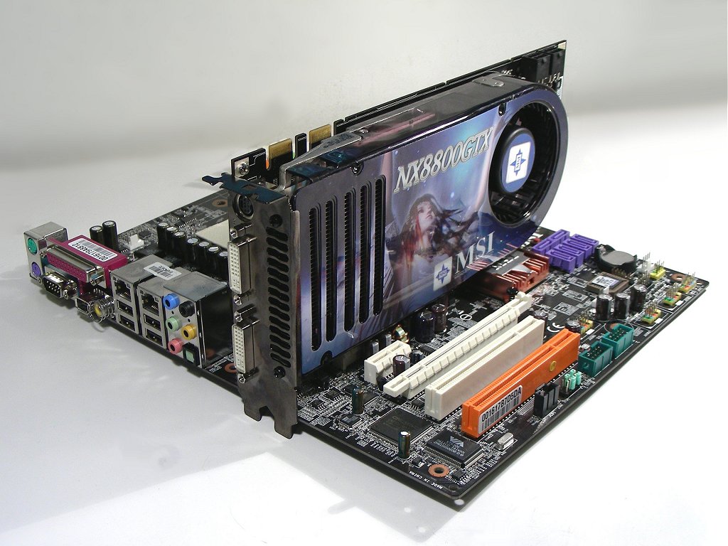
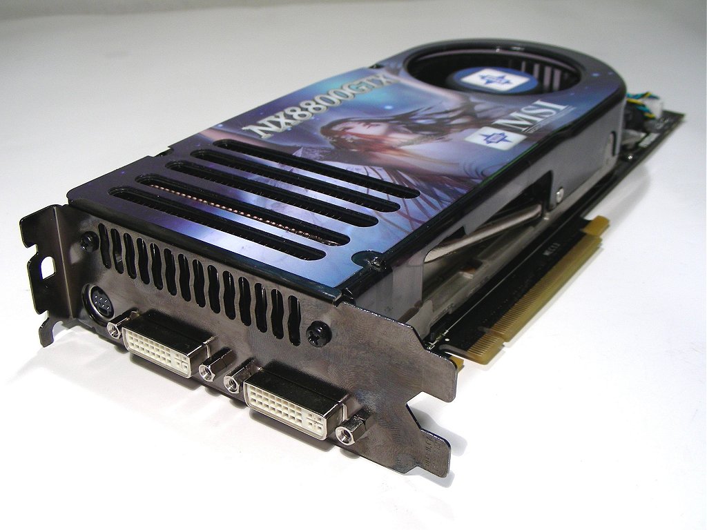
Nvidia is now mass producing what can only be considered weapon-grade silicon with their latest and greatest G80 GPU architecture (a.k.a. GeForce 8800). Currently the G80 is available in two mouth watering flavors, both of which are capable of blowing any existing competitor out of the water.
In fact, that could well be considered an understatement as we have already seen SLI 7900GTXs and CrossFire X1950XTX cards being defeated by a single GeForce 8800 graphics card. The GeForce 8800 GTX is the cream of the crop, featuring 768MB of on-board GDDR3 memory operating at 1.8GHz with a core clock frequency of 575MHz. And while all this sounds fairly typical of a high-end graphics card (the large memory capacity, high memory and core frequencies), the G80 architecture is like nothing we have encountered before.
The GeForce 8800 GTX brings a shift in GPU functionality and capability, moving away from the traditional pixel and vertex shaders we had got familiar with, to a collection of floating point processors also called Stream Processor Units (SPUs), this version uses 128 SPUs clocked at 1.35GHz. Then we have TAUs (Texture Address Units) of which the 8800 GTX features 32, along with 24 ROPs (Rasterization Operator Units).

The 8800 GTX utilizes a total of six 64-bit memory controllers operating in tandem, effectively creating a 384-bit wide memory bus. This 384-bit wide bus is connected to the 768MB GDDR3 memory operating at 1.8GHz. This means the 8800 GTX has a total of 86.4GB/s worth of memory bandwidth at its disposal, or theoretically 35.2GB/s more than the 7900 GTX.
There is also available the GeForce 8800 GTS which is the cut down version of the GTX, featuring less SPUs, TAUs and ROPs. Furthermore, the GTS version features less memory along with a narrower memory bus, lower memory and core frequencies.
Today we'll be looking at the more powerful, more expensive and slightly more exciting GTX version of the GeForce 8800 series as we take a peak at MSI's take on the latest generation graphics technology from Nvidia. The G80 is an impressive achievement for so many reasons; for one this new generation of graphics cards was not just paper launched. Rather, as the announcement was taking place and reviews appeared online, boards based on the GeForce 8800 chip also made their appearances in retail and online stores. Manufacturers were quick to deliver most likely wanting to take some advantage of the holiday season sales, though all shipping cards closely resemble Nvidia's reference design.
The G80 is arguably more complex than Intel's recently released Core 2 Extreme X6800 quad-core processor. Featuring 681 million transistors, the GeForce 8800 is the most complex GPU ever created. Just compare those figures to the X1900 XTX's 384 million transistors or the 7900 GTX's 278 million.
And while all these large numbers are quite mind blowing, it was not until we discovered that the G80 still uses the "old" 90nm design process is that we were completely blown away. This means that where Nvidia previously fit 278 million transistors for the 7900 GTX core, they have now managed to fit two and a half times more transistors.
While we do not know the exact size of the core, it certainly doesn't appear to be two and a half times bigger. The core is covered and protected by a heatspreader that cannot be removed without destroying the graphics card.
What we have done for you is dismantled this MSI GeForce 8800 GTX card to give you a clearer picture of what we are talking about. These images are available on the next page so be sure to check them out. Although the MSRP for the GeForce 8800 GTX is $599, this MSI card is currently retailing for around $650, though we are confident this price will fall eventually. The question now is what has MSI done to attract your attention away from the competition and focus it on their product? Let's move on to find out...
