A-Series Core Design, Cache Spec
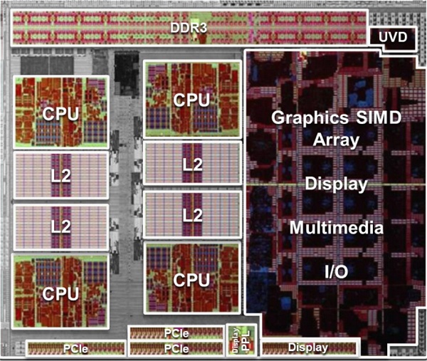
As mentioned earlier, Llano's Husky cores are based on the same K10 architecture used by the current Phenom II and Athlon II processors. However, the design is more closely related to the Athlon II, as Llano also abandons L3 cache. Instead, AMD decided to increase the L2 cache. Whereas quad-core Athlon II and Phenom II have 2MB of L2 cache, the A8 and A6-Series APUs receive 4MB – 1024KB per core.
Although the Phenom II's 6MB L3 cache increases performance in certain situations, it also elevates power consumption and essentially ruins the efficiency of these chips. Whereas the smaller dedicated L2 cache can be enabled or disabled as the cores are needed, the entire L3 cache stays awake even when only one core is being used. Apparently, AMD felt the performance tradeoff simply wasn't worth it.

Despite dropping the L3 cache, Llano's transistor count is still greater than any of its predecessors, including the hexa-core Phenom II X6 processors. In fact, it is possible that the Llano's transistor count is even greater than that of Intel's hexa-core Core i7 Gulftown processors as well, which is incredible. This makes the budget orientated Llano APUs extremely complex and it also makes the die area rather large.
The die area of the quad-core APUs for example is 228mm², which is larger than the high-end Sandy Bridge Core i5 and Core i7 processors' 216mm² die. Meanwhile, the more affordable Core i5 and Core i3 dies measure just 149mm². Naturally, larger dies cost more produce, and considering the Llano APUs are around 50% bigger than their competition, we have no doubt this will cut into AMD's bottom line.

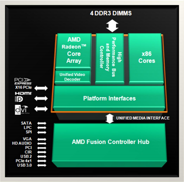
That said, what AMD has managed to achieve here is nothing short of incredible, especially when you look at processors and platforms from just a few years ago. AMD has taken a 66mm² (13w) northbridge, 200mm² (65-95w) quad-core processor, 108mm² (30w) graphics processing unit – what were once three entirely separate components – and merge them into a 228mm² (65-100w) A-Series APU.
