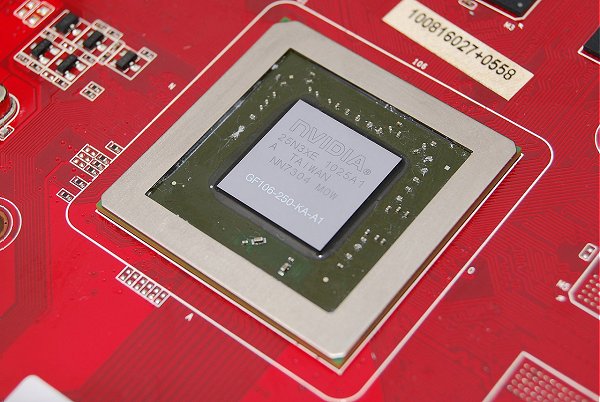
GeForce GTS 450 GPU in Detail
The GeForce GTS 450 is based on Fermi's third-generation Streaming Multiprocessor architecture. The graphics processor boasts 192 CUDA cores, the same shader power of the GT200 architecture used by the GeForce GTX 260 and thus, 43% fewer cores when compared to the GeForce GTX 460.

The GeForce GTS 450 features 32 TMUs (Texture Mapping Units), again 43% less than the GeForce GTX 460 and half than the older GeForce GTX 260. The 16 ROPs (Raster Operations Pipelines) on the GTS 450 are 33% less than the 768MB version of the GTX 460 and 50% less than the 1GB version.
The GTS 450's clock speed for fixed function units is 783MHz, while the CUDA cores operate at a more aggressive 1566MHz. These frequencies are the highest of any GeForce 400 series graphics cards available, though it's not uncommon for the budget cards to receive frequency boosts as it's cheaper to make a less complex GPU and simply overclock it.

The GeForce GTS 450 is said to become available in both 1GB and 2GB capacities, though we believe most cards will stick to the 1GB memory buffer. The memory is clocked at 900MHz (3600MHz DDR). Regardless of memory capacity the bandwidth will be limited to just 57.6GB/s due to the implementation of a 128-bit bus.
At least on paper for now we learn that the Thermal Design Power rating of the GeForce GTS 450 is very reasonable compared to previous GeForce models based on the Fermi architecture. Whereas the TDP of the GeForce GTX 460 (1GB) is 160 watts, the GeForce GTS 450 has received an even lower rating of 106 watts.

The GeForce GTS 450 draws in power from the PCI Express slot and from a single external PCI Express power connector. The GTS 450 requires one 6-pin connector, which is the same configuration used by the Radeon HD 5770. The GeForce GTS 450 also features a single SLI bridge connector allowing it to be paired with another graphics card for 2-way SLI which we will be testing in this review.
