Samsung announces backside power delivery network breakthroughs - what does it mean for...

Jimmy2x

Posts: 239   +29
Staff
Through the looking glass: Many advances in semiconductor technology hinge on reducing package sizes while incorporating added functionality and more efficient power delivery methods. Present methods of power delivery consume significant space on the wafer, leading to increased costs, larger die sizes, and fewer transistors. Earlier this year, Samsung Semiconductor presented its research on an alternative to conventional semiconductor power delivery methods: backside power delivery. This could lead to significant reductions in die size and decreased routing congestion.

According to a report from TheElec and Samsung's presentation at this year's Very Large Scale Integration (VLSI) Symposium, the semiconductor manufacturer used new backside power delivery network (BS-PDN) approaches to successfully reduce the required wafer area by 14.8% when compared to traditional front side power delivery networks (PDNs).

The successful implementation also yielded 10.6% and 19% area reductions in two ARM circuits while reducing wiring length by 9.2%.

In traditional frontside PDNs (FSPDNs), semiconductor components must be arranged on the front side of the wafer in order to provide transmission from the power line to the signal line and to the transistors.

This configuration requires shared space and resources between the delivery and signal networks, increasingly resistant routing to carry electrons across the back-end-of-line stack, and can result in energy loss during transmission to ground rails in the semiconductor structure.

BS-PDN (Backside Power Delivery Network) is designed to address these architectural and power delivery limitations. The approach completely decouples the power delivery and signal networks and uses the backside of the wafer to accommodate power distribution. Using the backside of the wafer, Samsung and other semiconductor manufacturers can instead direct power delivery through shorter, wider lines that offer less resistance, improved power delivery performance, and reduced routing congestion.

While the move from FSPDN to BS-PDN sounds promising, there are several challenges that prevent it from becoming a standard approach for manufacturers pursuing the technology.

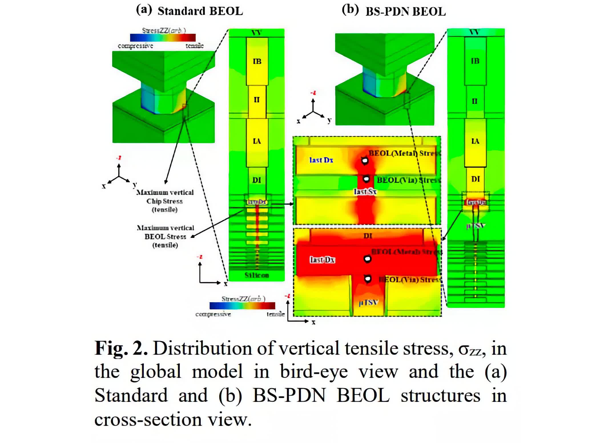
One of the biggest challenges to implementing the new power delivery model, also presented by Samsung at the symposium, is the potential reduction in tensile strength associated with BS-PDN. When applied, BS-PDN can reduce the tensile stress acts and through-silicon via electrode (TSV), resulting in separation from the metal layer.

Samsung said that this problem can be solved by reducing the height or widening the TSV, however more research and testing is required before a solution can be formally announced. Additional advances in signal and power line connectivity will also be required to successfully apply BS-PDN.

In addition to the above, advances in chemical mechanical polishing (CMP) technology would also be required. Current CMP implementations are used to remove 5 to 10 microns of "peaks and valleys" from the backside of a wafer. Implementing BS-PDN could require a new way to polish the wafer without damaging the underlying power components.

Samsung does not have a current timeline outlining official implementation of BS-PDN-based architectures, but based on current findings and challenges, it's not yet clear if we'll see BS-PDN implementations from Samsung, or other manufacturers like TSMC and Intel, for several more years.

Image source: imec-int.com

Permalink to story.

 
“…it's not yet clear if we'll see BS-PDN implementations from Samsung, or other manufacturers like TSMC and Intel, for several more years.”

How is this different from Intel’s PowerVia slated for late 2024 / early 2025?
 
The link above to BS-PDN is worth a check out

This idea has to have been around for a long time - so many smart people - so obvious - Maybe as stated just waiting the tools etc to catch up

I suppose the ultimate is on some super nano scale where data and power are the same - Information in physics no matter how small is energy
 
I'm sure it's very clever but the marketing people need firing. Backside power delivery just sounds like an alternative to waterboarding.
 
I suppose the ultimate is on some super nano scale where data and power are the same - Information in physics no matter how small is energy
To be more precise, storing or transferring information requires energy, but information and energy are otherwise nearly unrelated. There are many systems in physics -- from a quantum ground state to the eventual heat-death of the universe -- that contain information, but no free energy.

On a more pragmatic basis, I'll note power delivery systems like the decades-old D1W (Dallas one-wire) that extract power to components using the excess power contained in each bit pulse.
Let's say the physics is in a flux - see Maxwell Demon

Plus it's one of those intrinsic things - ie you can not separate information and energy
like Time as a concept has no meaning outside Space - as Einstein showed - speed of light is the same in a vacuum - no matter the view point or the speed you travel - so space has to distort, and there is no absolute measure of time
 
“…it's not yet clear if we'll see BS-PDN implementations from Samsung, or other manufacturers like TSMC and Intel, for several more years.”

How is this different from Intel’s PowerVia slated for late 2024 / early 2025?
PowerVia is an implementation of backside power delivery. It's on the 20A roadmap for the near future (def not several years away, at least on paper). Bear in mind there are clearly still timing uncertainties around this.

If you want to know more about the topic, it's worth looking at Applied Material's presentation from last year. https://ir.appliedmaterials.com/events/event-details/New-Ways-to-Wire-and-Integrate-Chips
IMEC was also talking BS-PDN back in 2021... Imec demonstrates critical building blocks for a backside power delivery network

And reports about Blue Sky Creek put implementation in 20A as more likely to be ready for HVM than not, but we shall see...
 
Back