Samsung wants to bring chips with glass substrate to the market, and fast

Alfonso Maruccia

Posts: 1,025   +302
Staff
In context: Manufacturers are trying to develop novel chip substrate technologies to save Moore's law and keep crunching the Megahertz rates up. Glass is the most promising material for next-gen substrates Manufacturers should start using them earlier than anticipated – if Samsung can succeed at its ramped-up R&D effort.

According to rumors from unnamed industry insiders, Samsung has decided to invest heavily in the research and development of glass substrates for chip manufacturing. The company plans to bring products to customers by 2026, creating a "coalition" of subsidiary organizations to speed up technology development.

The leakers say that three divisions within the Korean conglomerate – Samsung Electro-Mechanics, Samsung Electronics, and Samsung Display – will develop the new glass-based chip substrates. Samsung Electronics will work on integrating semiconductor components with the new substrates, while Samsung Display and Electro-Mechanics focus on the glass processing part.

The insiders said that Samsung will try to leverage a synergic approach among its subsidiaries, leveraging their expertise in their respective fields. During the Consumer Electronics Show 2024, Samsung Electro-Mechanics announced plans to build mass-production capabilities for glass substrates by 2026.

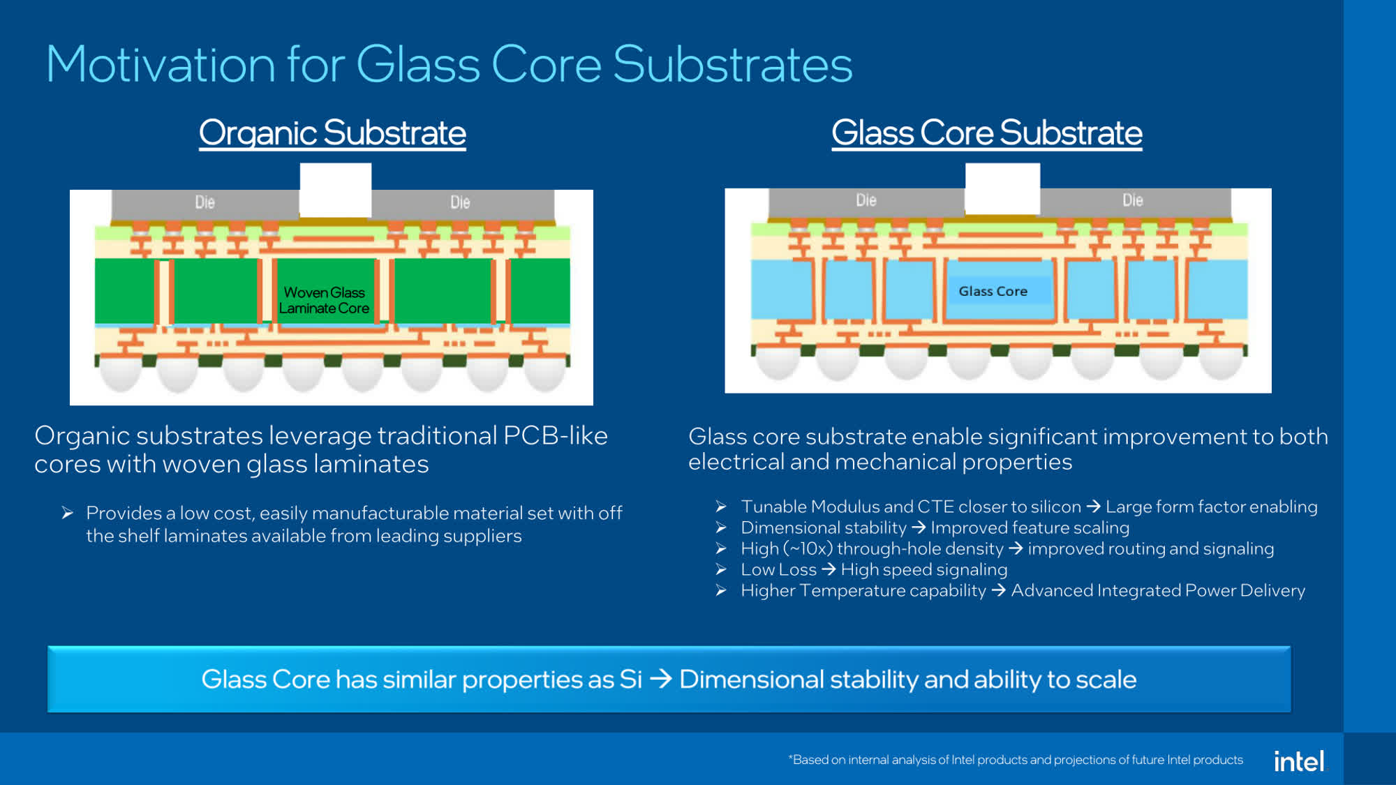
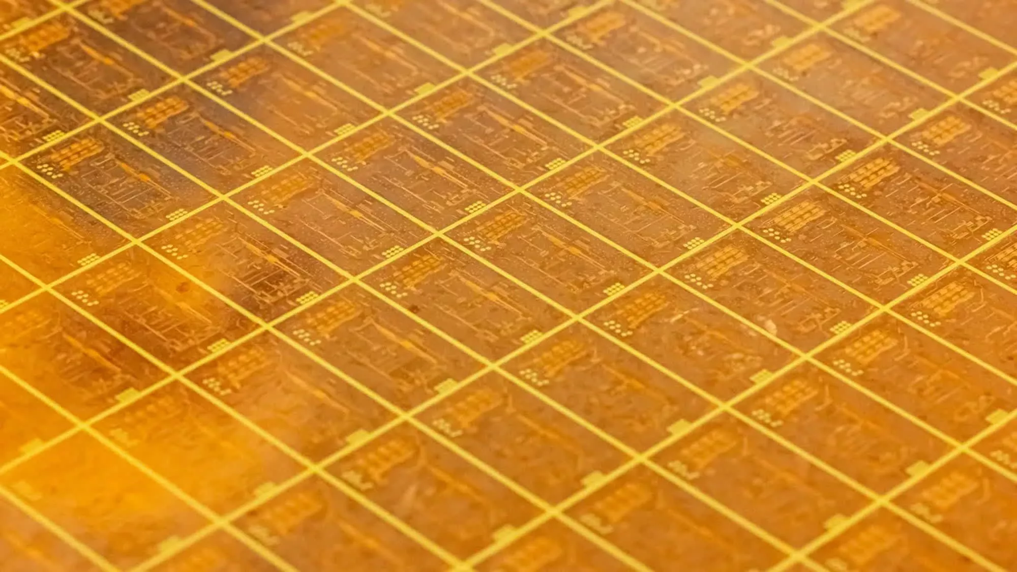
Glass substrates can theoretically bring significant improvements to the chip manufacturing process. Compared to traditional organic substrates, glass shows an enhanced flatness that improves the depth of focus for lithographic processes. The material also has higher dimensional stability for interconnects and provides higher thermal and mechanical strength.

The material could withstand higher temperatures and stress levels, making chips more durable and resilient even in "harsh" data center conditions. The technology would be ideal for multi-chiplet, system-in-package (SiP) applications, which are set to become one of the industry's most popular chip designs. Intel has been developing a glass substrate solution for years, and the company recently announced its plans to launch novel commercial products by 2030.

Samsung and Intel aren't the only companies working on the next generation of substrate technology. Japanese manufacturer Ibiden has also joined the R&D effort for glass-based designs, while South Korean company SKC has opened a new subsidiary (Absolics) to develop new mass production capabilities. Absolics has already partnered with AMD and other leading semiconductor companies.

Permalink to story.

 
It's kind of disingenuous when people/companies say they are changing over to "glass" which will be "revolutionary"...

Silicon is basically sand... and what is glass? MELTED SAND!!

It's really not that revolutionary...
 
It's kind of disingenuous when people/companies say they are changing over to "glass" which will be "revolutionary"...

Silicon is basically sand... and what is glass? MELTED SAND!!

It's really not that revolutionary...
The (silicon) chips are bonded to a substrate -- current substrates are organic: multiple active layers between passive resin layers. Glass substrates are indeed something new to the industry. Whether you wish to label it 'revolutionary' or not is at your discretion.
 
It's kind of disingenuous when people/companies say they are changing over to "glass" which will be "revolutionary"...

Silicon is basically sand... and what is glass? MELTED SAND!!

It's really not that revolutionary...

Sure, it’s so simple, it’s only taking a decade of R&D to maybe make it work.
 
It's been a long time since this came to light, I wonder if it's already feasible or we're in the same situation as batteries where they set a target in the hope of delivering the proposed product.
 
It's kind of disingenuous when people/companies say they are changing over to "glass" which will be "revolutionary"...

Silicon is basically sand... and what is glass? MELTED SAND!!

It's really not that revolutionary...
I could not have said this better.

However, the failure of explanation in the article(which is not the fault of Techspot staff) is as follows: What the article is trying to say is that instead of strained pure silicon(which is expensive and difficult to make), the substrate materials will be made of more common forms of glass that are equally structurally and mechanically stable but MUCH less expensive and very much easier to make. This will have the effect of making chips less expensive, easier and faster to manufacture.
 
...the substrate materials will be made of more common forms of glass that are equally structurally and mechanically stable but MUCH less expensive and very much easier to make. This will have the effect of making chips less expensive, easier and faster to manufacture.
100% incorrect. The purpose of the substrate isn't simply to provide a stable base, but to route thousands (soon to be tens of thousands) of signal and power connections from the chip to the exterior world. Glass doesn't conduct electricity, so these so-called "glass substrates" are actually dozens of ultra-thin glass layers bonded between metal ... an extremely difficult task to do stably. Furthermore, the final sandwiched product must have a modulus of elasticity and coefficient of thermal expansion very similar to strained silicon, AND also be able to conduct away vast quantities of heat -- a difficult task for pure glass, given its low thermal conductivity.

There is nothing "much less expensive and way easier to make" about glass substrates ... which is why companies like Intel have spent a decade of R&D attempting to develop it ... and still have a few years left to go.
 
Back