For the last 12 months, AMD has had the Radeon HD 6970 be its premier single GPU graphics card, competing head to head with the GeForce GTX 570 and at times challenging the mighty GTX 580. For about $369 today, you can still get one hell of a graphics card, comprised of 2.6 billion transistors, a die measuring 389mm2 and a 250W TDP rating, but most importantly capable of running all modern PC games fluidly except for some extreme scenarios.
When compared to its previous generation board (the Radeon HD 5870), the Radeon HD 6970 was on average 24% faster. Now a year later AMD is launching its Radeon HD 7000 series which has been given the codename 'Southern Islands'.
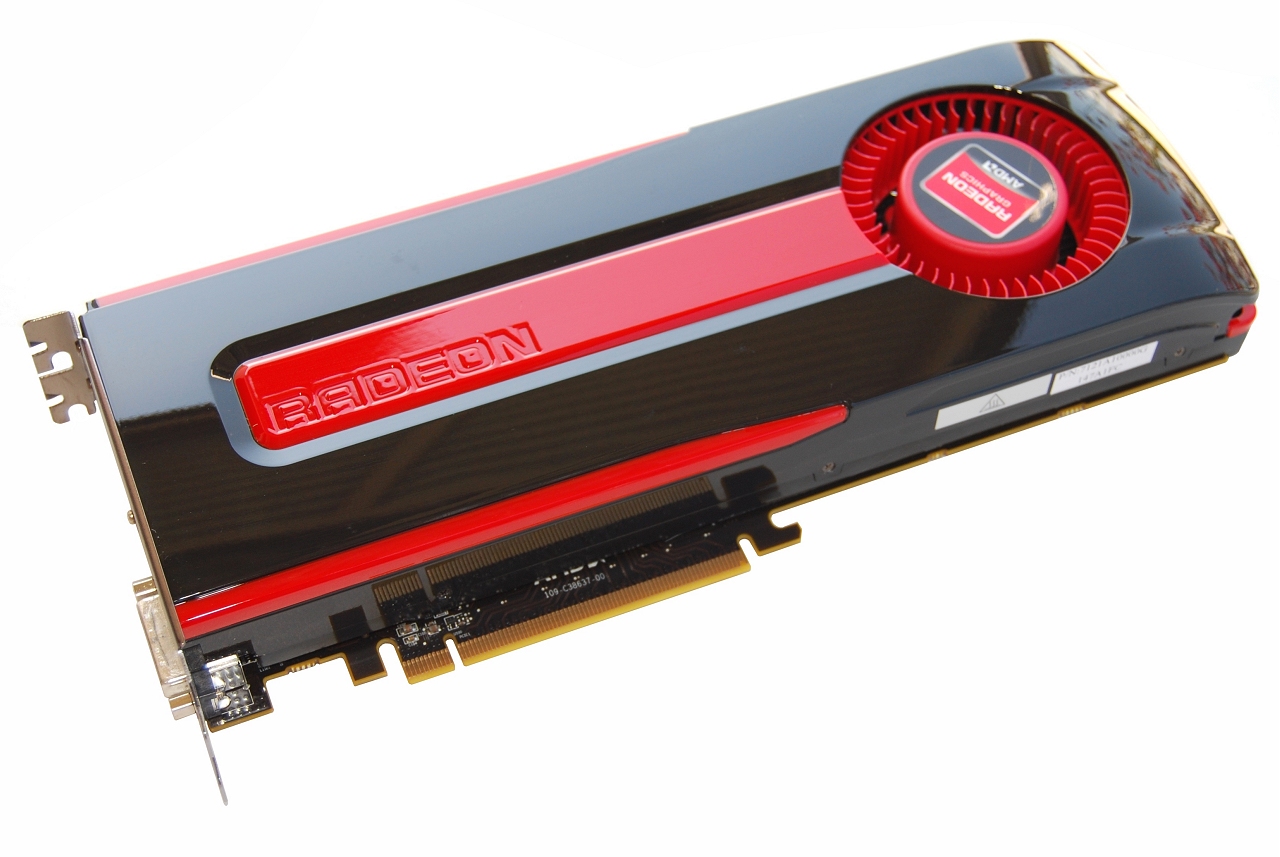
The Radeon HD 7970 is the first of a series of upcoming graphics cards that are making the jump to the 28nm fabrication process. The new HD 7970 will effectively become AMD's new flagship single GPU graphics card come January, when the board is expected to ship.
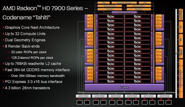
The die shrink means AMD can cram more transistors into the same space, a lot more. Although the die size is only slightly smaller, at 365mm2 there are some 1.7 billion more transistors, taking the total count to a whopping 4.3 billion. This number whales that of the GeForce GTX 580 which boasts 3+ billion transistors in its massive 520mm2 die.
Nvidia is said to be updating their graphics lineup early in 2012, with the GeForce 600 series also expected to utilize the 28nm process. In an effort to beat Nvidia, AMD pushed up their (soft) launch date to late December.
With a mere two weeks before it'll be possible to get your hands on a new Radeon HD 7970 graphics card, it's definitely nice to get a look now at how they perform. But before we jump into our gaming benchmarks, let's take a moment to check out the new card's capabilities and features in greater detail.
The Radeon HD 7000 series is a big leap for AMD, representing its most significant architecture overhaul in the last decade. It was back then that AMD adopted the Graphics Parallel Core architecture, which employs groups of scalar processors that work out very long instruction words, commonly abbreviated as VLIW.
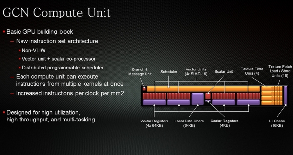
The Radeon HD 5000 series used the VLIW5 architecture, while last year's 6000 series transitioned to a more advanced VLIW4 architecture. However, the Radeon HD 7970 and all other graphics cards based on the high-end Tahiti core replace the VLIW stream processor clusters with what AMD calls GCN (Graphics Core Next) compute units.

A GCN is basically a GPU that can handle both graphical and computing tasks with a high level of efficiency. It's AMD's answer to Nvidia's Fermi architecture, making the Radeon HD 7970 a capable computing workhorse. It's worth noting that only high-end HD 7000 series cards are based on the new Graphics Core Next architecture, while all other models will still use VLIW.

So essentially, a Shader cluster is now called a GCN compute unit and each unit is a super-scalar processor with scalar and vector elements that follow a new non-VLIW instruction-set architecture. This is a more efficient architecture that delivers more power per millimeter square of GPU die area.

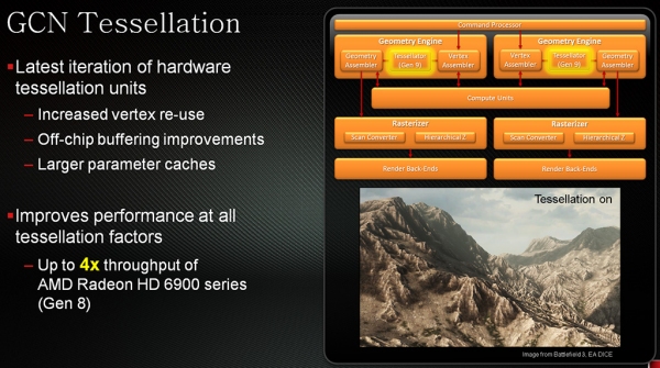
The HD 7970 features a new 9th Generation Tessellation Geometry Engine with optimizations such as increased vertex re-use, off-chip buffering improvements and larger parameter caches. This helps improve performance at all tessellation factors with up to 4x the throughput of the HD 6900 series (Gen 8).
