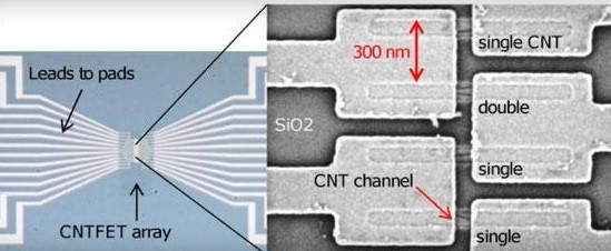
Scientists at IBM’s T.J. Watson Research Center in Yorktown Heights, N.Y. are making substantial progress on what is expected to be the successor to silicon-based microprocessors. Carbon nanotubes have been arranged on the surface of a silicon wafer to create a hybrid chip with more than 10,000 working transistors.
Researchers have become increasingly concerned with the possibility that Moore’s Law – the idea that the number of transistors on a chip can be doubled every 12 to 18 months – might fail sooner rather than later.
IBM says the breakthrough is significant and worth getting excited over. Silicon has been an incredibly resilient building block over the past 50 years or so but scientists have yet to find a solution beyond the next few generations.
Carbon nanotubes are expected to allow chip makers to build smaller transistors that can turn on and off much more quickly than their silicon counterparts. Supratik Guha, director of physical sciences at IBM Research, said his group suspected carbon nanotubes would outperform any other switches made from any other material. Simulations performed by device physicists showed a factor of five or more improvement over conventional silicon devices.
The processor industry as a whole has hit a wall in recent years in terms of overall clock speed. This has forced the industry to shift gears and build multi-core processors to help tackle workloads rather than continuing to ramp up clock speeds.
Once the new technology has been fully perfected for use by the end of this decade, scientists anticipate future processors will feature much higher clock speeds in addition to even more transistors being crammed onto a single wafer.
")