Forward-looking: The explosive growth of artificial intelligence (AI) has shifted the semiconductor technology race into overdrive. Yesterday, Intel announced the arrival of its extreme ultraviolet (EUV) Intel 4 technology at Fab 34 in Ireland. The highly anticipated milestone leaves Intel positioned to deliver on its promise of delivering five new process nodes over the next four years.

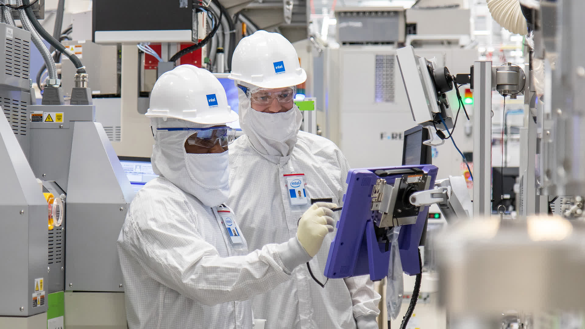
The heavy computing requirements of AI push evolving manufacturing processes that shrink overall chip sizes while allowing a higher concentration of compute elements on each chip. As a result, companies like Intel, TSMC, and Samsung are constantly investing in facilities, equipment, and resources to stay one step ahead of the competition in the semiconductor market. On Friday, Intel announced the arrival of its Intel 4 manufacturing process, a vital component of the company's upcoming Intel Core Ultra processor lineup, at its Fab 34 manufacturing facility in Leixlip, Ireland.
Intel 4, previously known as the 7nm process node, will reportedly provide upwards of a 20-percent increase in clock speed while significantly reducing power consumption. It brings an overall increase in yield due to the decreased die size. The new manufacturing process improves Intel's current Intel 7 (10nm++) process node currently powering the 12th gen Alder Lake family of CPUs and the 13th and upcoming 14th gen Raptor Lake processors.
The new manufacturing process relies on the latest extreme ultraviolet (EUV) lithography systems from ASML. The EUV systems are roughly the size of a small shipping container and support high-volume production of nodes as small as 7nm to 5nm. Its latest TWINSCAN NXE:3400C can produce upwards of 170 wafers per hour.
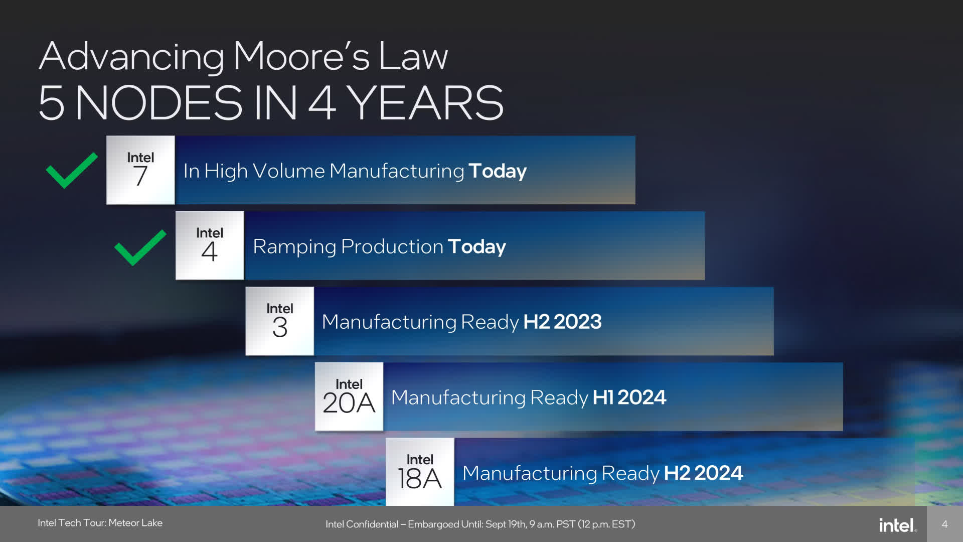
Intel's transition to the Intel 4 manufacturing process is a huge step forward on the company's four-year roadmap. If it can stay on pace, the company will move to the Intel 3, 20A, and 18A processes in the coming years.
The new capability will undoubtedly help Intel gain ground in the already competitive, sometimes contentious, semiconductor race. Earlier this year, Intel argued that US companies should be eligible for higher CHIPS Act subsidies than those owned by foreign companies such as TSMC. The Taiwanese chip giant asserted that allocating grants based on a company's registered headquarters location was an inefficient and inaccurate distribution method. Both manufacturers were later hushed by Commerce Secretary Gina Raimondo, stating that the program's focus was strengthening national security and not to boost struggling chipmakers.
https://www.techspot.com/news/100337-intel-latest-high-volume-euv-chip-production-could.html
