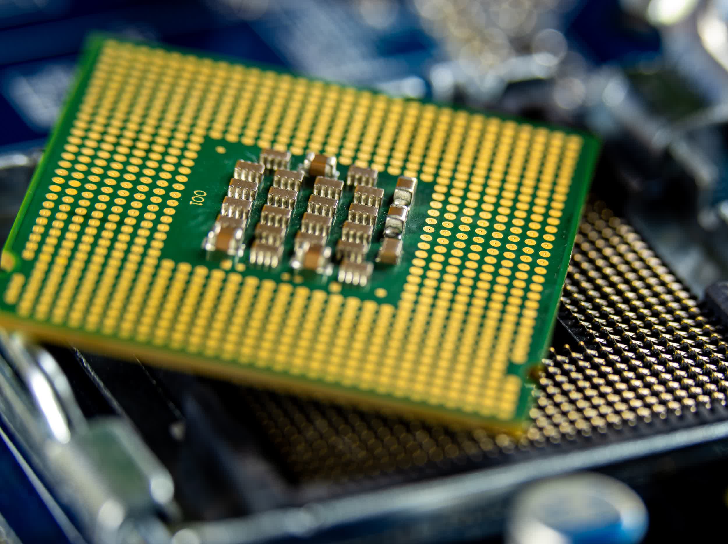
In brief: Japan is looking to become a major player in the race to commercialize the next generation of chip technology and will partner with the US to realize its goal. According to a report from Nikkei Asia, private companies from the two countries will work together on research and mass production.
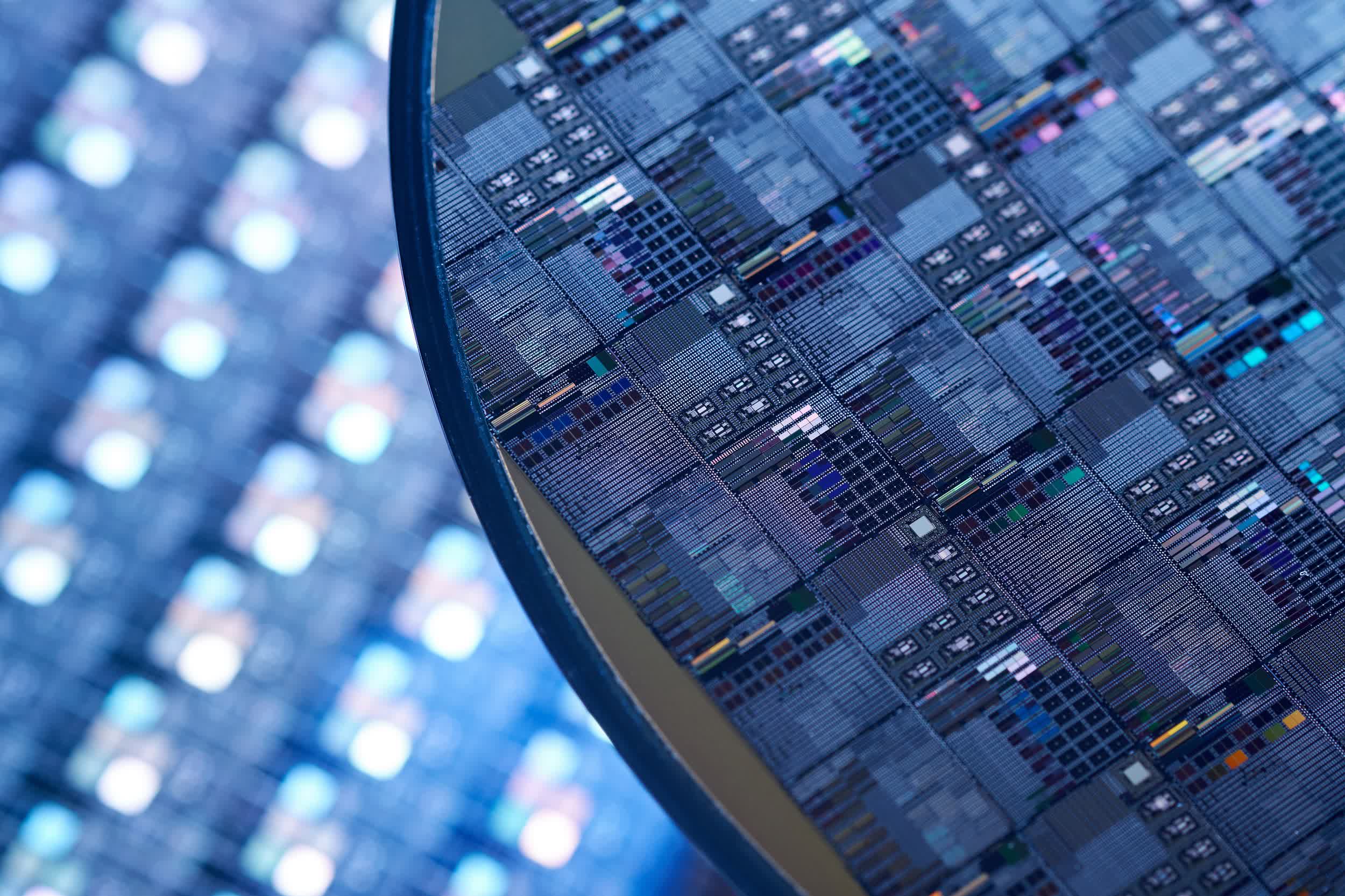
Each side has plenty to bring to the table. IBM, for example, showed off a 2nm design last year that could accommodate as many as 50 billion transistors on a chip the size of a fingernail. Japan, meanwhile, is home to several major chipmaking equipment makers including Canon and Tokyo Electron.
Joint research could begin as soon as this summer, and the first facility in the region is expected to be built between fiscal year 2025 and fiscal year 2027.
The publication notes that Japanese and US firms could establish an entirely new company to run the project, and that Japan's Ministry of Economy, Trade and Industry will partially subsidize R&D costs and capital expenditures.
According to Nikkei, the first wave of 2nm chips will likely be destined for data centers, quantum computers and flagship smartphones. They could also be useful in military applications, linking them directly to matters of national security.
Rival TSMC is widely regarded as the industry leader in next-gen chip production. The semiconductor giant is on track to start mass producing 3nm chips later this year and aims to have 2nm chips rolling off the assembly line by the end of 2025.
Image credit: Sergei Starostin
https://www.techspot.com/news/94957-japan-us-partner-2nm-chip-rd-manufacturing.html
