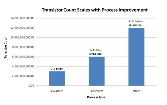
Moore's Law states that the density of a chip will double approximately every two years. Samsung has declared that the law is not slowing down to a halt for the company, disclosing details regarding the roll-out of 20nm process technology, which will enable the transistor count to roughly double yet again.
"Our focus for this process technology generation is to maintain the same increases in performance, power efficiency, and density that we've seen moving from 45nm to 32/28nm with the addition of High k Metal Gate (HKMG)," a company spokesperson said in a statement. "Our 20nm technology will be a full node shrink from 28nm, enabling the ~50% area scaling that the industry has come to expect with each technology generation. The technology has been designed to allow us to maintain our leadership in die size and cost, which remain critical factors for customers at leading-edge nodes."
The electronics giant also listed a few 20nm HKMG features:
- A build on the HKMG materials & integration concepts qualified at 32nm.
- Planar bulk CMOS technology will be used with second-generation gate last approach to HKMG.
- 193nm immersion lithography will be supplemented by source-mask optimization constrained minimum pitch to reduce the need for time-consuming, costly double-patterning.
- Second-generation ultra-low k dielectrics will be employed to lower power dissipation by reducing interconnect capacitance and wiring delay.
- Innovation with local interconnect and self-aligned vias to achieve cell-level scaling and elimination of a metal layer.
- Fifth-generation strained silicon technology will be integrated for power and heat reduction and more efficient switching.
- 30 percent improvement in performance over 28LP at the same standby current.
- The 20nm technology is ideally suited for a broad range of high performance and power-sensitive devices, including chips designed for smartphones, tablets, other portable consumer electronics as well as IT communications infrastructure.
Samsung is expecting test-chip shuttles for customers to start shipping in the second half of this year.
https://www.techspot.com/news/42571-samsung-talks-about-20nm-chips-tests-in-2011.html