Forward-looking: TSMC is continuing preparations for its 2nm-class manufacturing process technologies. The hardware is progressing well, while third-party companies and chip designers will need to adapt to the slew of innovations that N2 is bringing to the table.
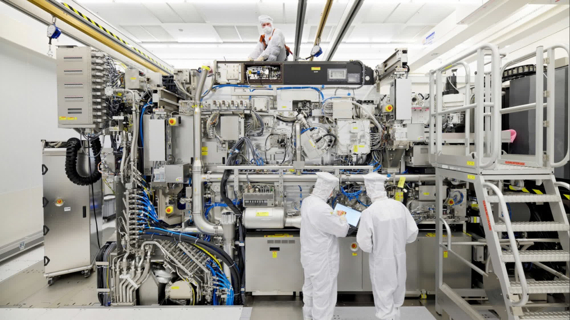
In the next few years, Taiwanese foundry TSMC will introduce some of the most advanced chip manufacturing technologies on the planet. The 2 nanometer-based N2, N2P, and N2X process tech will include multiple innovations, and the entire ecosystem orbiting around the company's silicon business is destined to change accordingly.
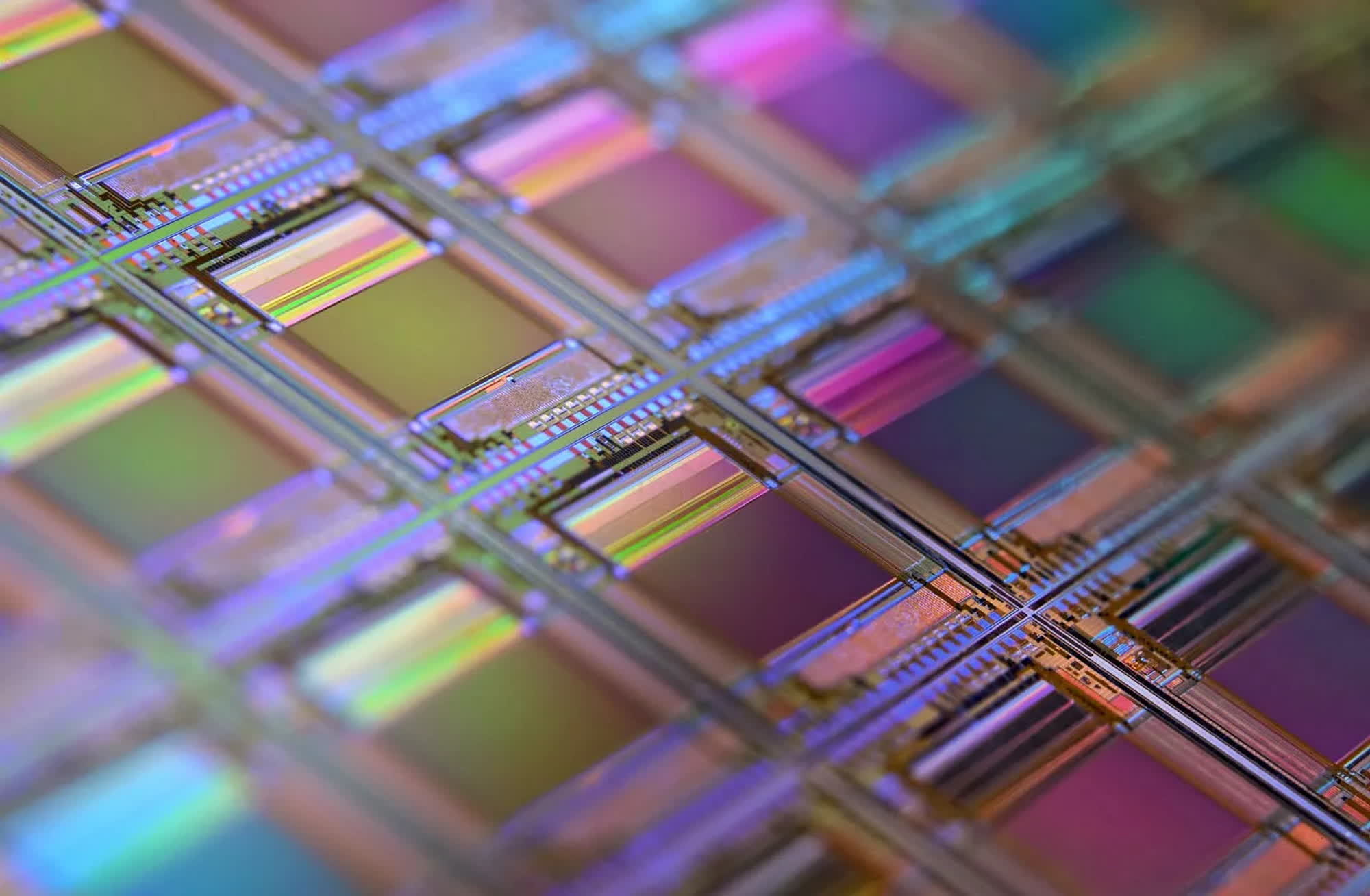
As noted by AnandTech, N2 and its future iterations should bring a lot of improvements to microchips, including a reduction in power consumption (-25-30%), more performance (+10-15%) and transistor density (>1.15x) in a "mixed" chip configuration (50% logic, 30% SRAM, 20% analog). Mass manufacturing of 2nm chips should arrive in the second half of 2025, but TSMC is working with its customers and partners 2 years in advance because the "nanosheet is different."
The N2 process will include innovations such as nanosheet gate-all-around (GAA) transistors, backside power delivery, and super-high-performance metal-insulator-metal (SHPMIM) capacitors. TSMC said during its latest Open Innovation Platform forum in Europe that to take advantage of such novel technologies, major chip designers need to use new electronic design automation (EDA) simulation, verification, and IP tools.
GAA transistors behave differently than FinFET ones, TSMC warned. Therefore, chip companies will have to start their design workloads essentially from scratch. Developing new IPs based on the 2nm process upgrade is not "harder," TSMC said, just different. Companies will have to adapt to the new tech, just like they went from planar transistors to a "3D" (FinFET) design in the past.
Major manufacturers of EDA software (Cadence, Synopsys) have already been certified by TSMC to work on N2, and chip developers can start using the new tools right away. The most complex part of the 2nm transition involves pre-built IP chip designs, because TSMC is still building some blocks to be included in the aforesaid designs.
Standard elements such as GPIO/ESD, PLL, SRAM, and ROM are ready both for mobile and high-performance computing (HPC) applications. Some components exist in form of pre-silicon development kits, while others have already been tested in actual hardware. Other N2 blocks such as non-volatile memory, interface IP, and chiplet IP are not available yet, which could bottleneck chip design efforts. Third-party companies such as Alphawave, Cadence, Credo, and eMemory are already working on them, TSMC said.
https://www.techspot.com/news/100481-tsmc-2nm-manufacturing-process-coming-along-but-take.html