Why it matters: The Pat Gelsinger-powered Intel has had great success with the launch of Alder Lake, but the company has big ambitions for the future. According to a patent that has recently surfaced online, Team Blue could use "stacked forksheet" transistors to keep Moore's Law alive.
By now it's no secret that Intel has been on a cultural transformation train under its new CEO Pat Gelsinger. The Team Blue boss is an outspoken and overly optimistic leader, and this has restored some investor confidence over the past year. With the successful launch of the company's first Alder Lake CPUs, Gelsinger believes AMD's Ryzen-powered conquest of the enthusiast desktop market may be coming to an end.
Beyond the hype, Intel needs time to recover its chipmaking crown which could take years. Over the past several months, the company has revealed several new process and packaging technologies that are in the pipeline, including new 3D transistors, Foveros logic-to-logic integration, and Embedded Multi-Die Interconnect Bridge (EMIB).

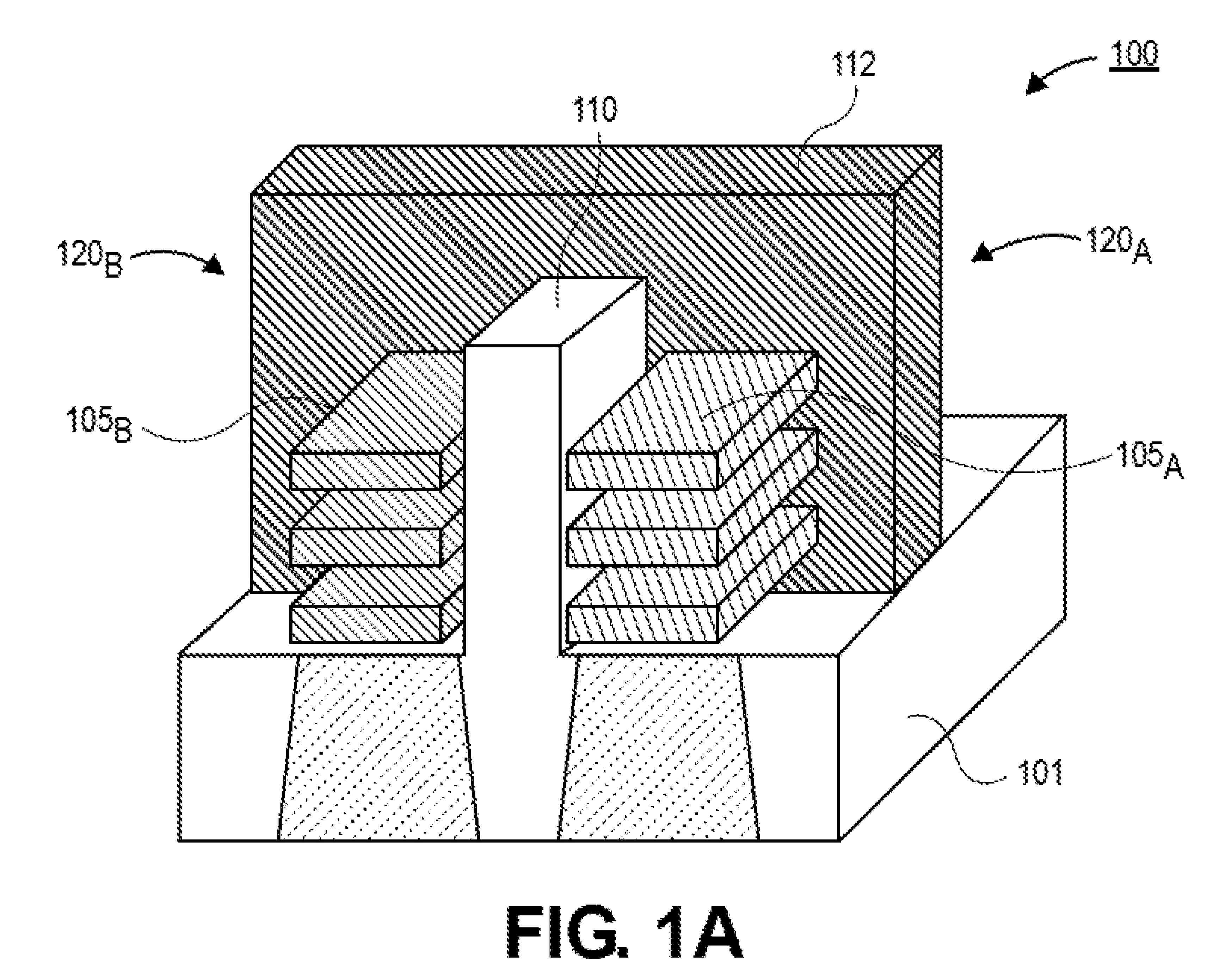
However, the most interesting aspect of Intel's aspirations to become a process leader can be found through its latest patents. One of these describes what Intel calls a "stacked forksheet transistor," which is key to keeping Moore's Law alive at sub-3nm process nodes.
The patent itself doesn't include any claims of Power-Performance-Area (PPA) improvements, but it does reveal how Intel envisions a vertically-stacked CMOS architecture that could enable higher transistor densities in future designs. This would come at a great cost in terms of manufacturing complexity, and Intel says further scaling down transistors requires a trade-off between the smallest size of a feature patterned in a semiconductor stack and the spacing between these features.

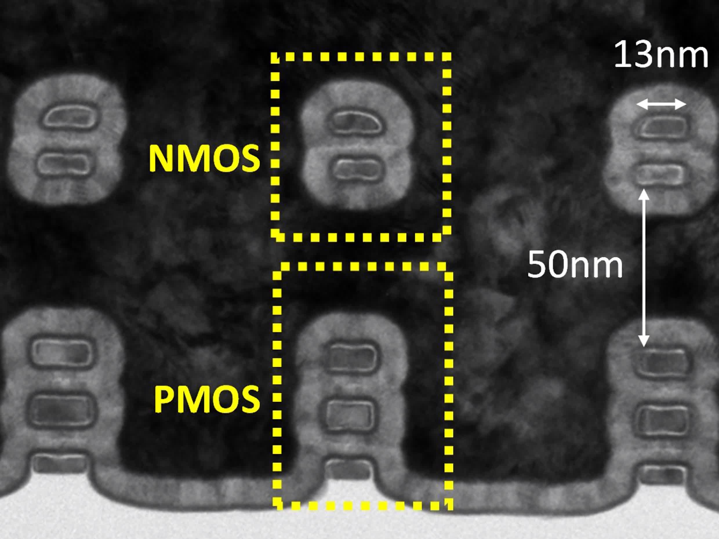
Intel is exploring the idea of using "nanoribbon" transistors that can be stacked on top of each other using a thin film of germanium that serves as a dielectric separation layer. This would allow the company to pack PMOS and NMOS transistors much closer together without affecting their operation. At the very least, this should lead to the reduction of the footprint of a simple CMOS device by half, so essentially a doubling of the density of future integrated circuits.
As noted by Tom's Hardware, a Belgium-based research group called Imec has also explored a similar concept dubbed complementary FET (CFET) and performed simulations on a 2nm process node. The results showed a 10 percent speed increase or a 24 percent improvement in energy efficiency over traditional nanosheet designs, coupled with a 20 percent reduction in cell area. Furthermore, this could reduce the footprint of a CPU's cache --- which usually takes up a huge chunk of die area --- by an even more impressive 30 percent.

This research was conducted in 2019, and the components built by Imec weren't entirely built out of nanosheet/nanoribbon transistors. Instead, they were made of a bottom FinFET layer with a single nanosheet on top, so it's entirely possible that Intel's version could achieve better results.
For reference, TSMC claims its upcoming 3nm process node will offer a 10 to 15 percent improvement in performance or up to a 30 percent increase in energy efficiency when compared to its 5nm process node. The foundry says the new node also enables up to a 70 percent improvement in logic density for CPU cores and a 20 percent improvement in terms of SRAM density.
Even though the road from patent to commercial applications isn't clear yet, the new patent offers a glimpse into what Intel's Components Research Group is doing to help Intel's ambitions around gate-all-around transistors for nodes like Intel 20A and beyond.
In the meantime, the company is busy expanding its manufacturing capacity and is planning to spend $25 to $28 billion in 2022 for that alone.
