When it comes to semiconductors, leading is not everything

Jay Goldberg

Posts: 75   +1
Staff
Editor's take: Undeniably, we usually spend a lot of time talking about leading edge semiconductor manufacturing. This is a common mistake that everyone falls into when discussing semis, one which we are as guilty of as anyone. The world is rightly focused on the scarcity of companies capable of operating at the leading edge, but there is a lot more to semis.

We recently went searching for data on fab capacity by process nodes, and everyone agreed that the leading expert on the subject is Bill McClane at IC Insights. He maintains one of the most rigorous models out there on the subject, and rightly charges a premium for his reports. This is must-read material for anyone planning out a multi-year semis roadmap.

Editor's Note:
Guest author Jonathan Goldberg is the founder of D2D Advisory, a multi-functional consulting firm. Jonathan has developed growth strategies and alliances for companies in the mobile, networking, gaming, and software industries.

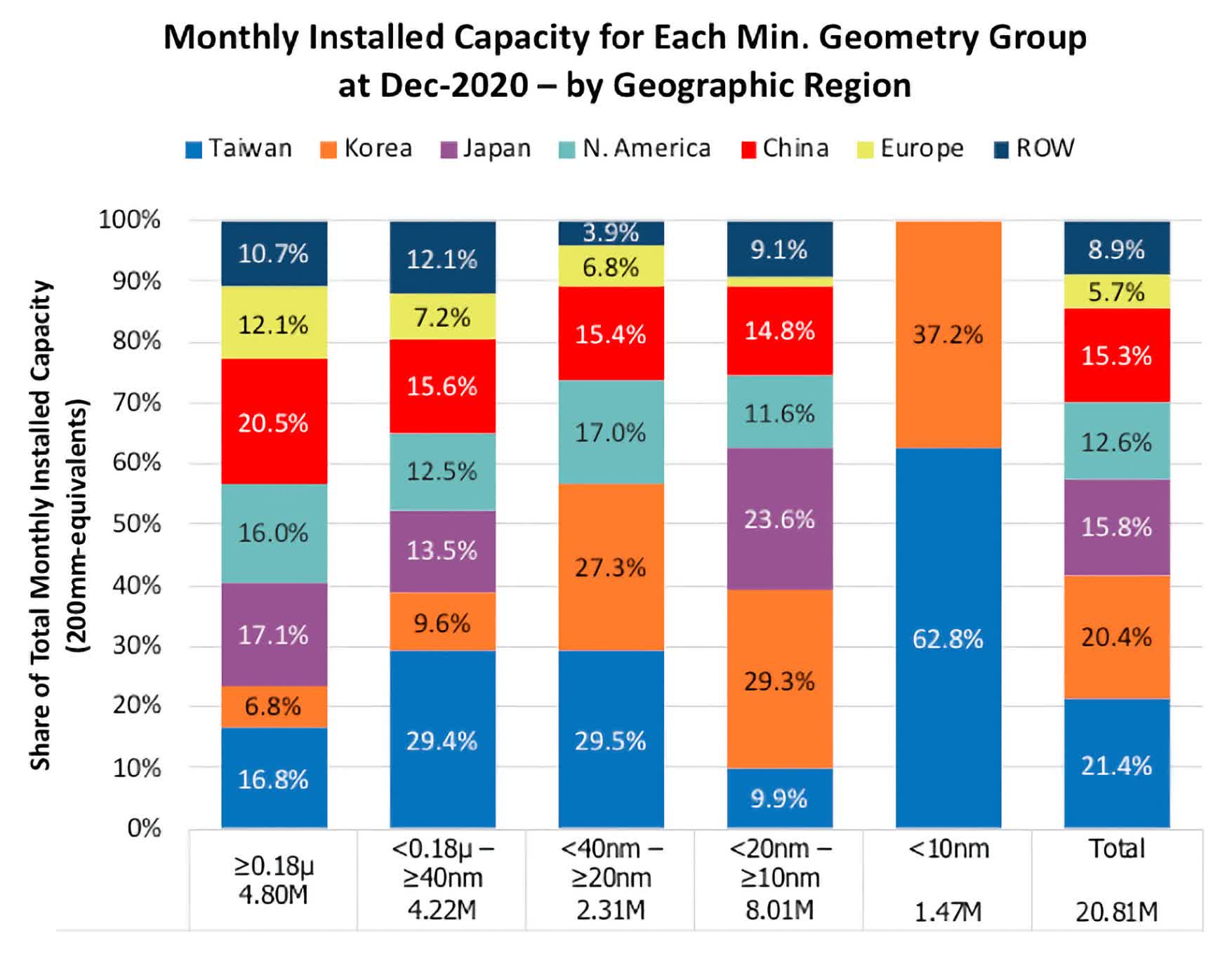
A quick Google search yielded this excerpt from IC Insight's data, and it tells an important story...

Over 90% of the world's semiconductor capacity is operating at 10nm or above. We can argue about where to draw the dividing line, but it is safe to say that the vast majority of capacity operates at the trailing edge.

This is important for a number of reasons.

First, when the world ran out of semiconductors in 2020/2021 – most of those shortages were occurring in these more mature processes. TSMC's leading customers were all able to get most of the capacity they needed at 7nm, but there was real pain for industrial and automotive customers.

These companies needed prosaic parts like microcontrollers (MCUs) and power management ICs (PMICs), and these products are generally produced at older nodes. Today, even as the supply shortages have turned to excess inventory in many categories, the older products are just catching up with the pent up demand from two years ago.

Secondly, the US government is currently struggling to decide how to allocate $52 billion of CHIPS Act funds. If the purpose of those funds is merely to bring leading edge processes back to the US, then go ahead and give all the money to Intel. They will dividend out $7 billion or $8 billion to shareholders and proceed with their plan to catch up on manufacturing that they would have to implement anyway.

On the other hand, if the goal is to truly secure the US semis supply chain, then perhaps a better plan is to divide that money up more broadly. Ideally, they would spend the money to plant a lot of seeds leading to new company formation and in basic academic research, which could then be commercialized by the private sector. Unfortunately, there are no easy mechanisms for doing this yet, and so another approach is to divide up the funds among a broad swathe of US companies involved in semis manufacture, so long as they commit to increases in US capacity. This does not just mean fabs and foundries, but also needs to include the tools companies, robotics providers and chemical makers – the whole supply chain. Intel should get some, but not the majority of those funds.

According to the Semiconductor Industry Association, the CHIPS Act has had a positive collateral effect by triggering the private sector into investing some $200 billion for US semiconductor production.

Finally, these numbers should remind us that the story is broader than just TSMC and Samsung. There is still a lot of interesting, important work being done at the trailing edge foundries.

The most obvious example of this is Global Foundries. GloFo is not at the lead in silicon manufacture but it has carved up some very sizable "niches" like silicon on insulator (SOI) and Silicon Carbide. And while they do not have the near duopoly on this that TSMC and Samsung enjoy with 7nm, they come close with many of their SOI lines. If for any reason the US ever lost access to TSMC, GloFo would arguably be as important a part of the solution as Intel.

Permalink to story.

 
There is still plenty of life in these older processes, things like ardinos and raspberryPis have shown that there is nothing wrong with 10nm or even larger nodes. We've reached a point where running bleeding edge hardware isn't noticeable unless you have specific work loads. I'd even argue that midrange hardware from several generations ago is fine for people who want to do light gaming. My 1800X+1070ti I had was running ESO at 90-100FPS no problem. Most people use PCs for browsing the internet or watching youtube. I even know plenty of people who don't even have a PC or laptop in their house anymore, they've replaced it with their phones.

There is still plenty of life in these older processes and AMD has even proven that with their chiplet design by mixing different nodes on the same CPU to reduce costs. Many compute units simply don't benefit from smaller nodes anymore. I would also like to add that as much as I hate "the cloud" it has replaced many functions for many people that would otherwise be done on a home PC. As internet speeds get faster and faster more functions will be off loaded into the cloud
 
This is misleading, as (though it's unclear from the chart shown) IC Insights appears to be basing capacity on wafer starts. But ultimately, companies are buying transistors, not wafers-- and a 5nm 200mm wafer has 16X the transistors of a 20nm wafer. Transistors that run much faster too.

Based on the actual amount of transistors supplied, the 12nm and larger nodes don't supply anywhere near 90% of the market.
 
I can't believe I read this. Wasting time and money to create something that already exists and is protected by thousands of patents? Even if this barrier did not exist, it would take so long to create a usable manufacturing process that the technology would already be retrograde even for less demanding industries, it is much simpler and more efficient to give subsidies to companies like Samsung and TSMC to expand their factories.

It is better to suggest that they should just burn the money.
 
CHIPs act led to bigger executive bonuses and then firing employees. Safe to say that's not what a healthy government would have wanted.
 
CHIPs act led to bigger executive bonuses and then firing employees. Safe to say that's not what a healthy government would have wanted.
Why spread misinformation? Intel's Gelsinger received roughly 1/5 the compensation in 2022 that he did in 2021. NVidia's Huang received a $4M bonus ($1M more than the prior year) ... but then NVidia hasn't announced any layoffs at all. Texas Instrument's CEO Ilan (who just stepped into that role from VP) will get a compensation bump, but it'll be less than what the old CEO earned. And Micron's Mehrotra recently announced that senior executives, including him, will receive a pay cut and no bonuses this year.
 
Why spread misinformation? Intel's Gelsinger received roughly 1/5 the compensation in 2022 that he did in 2021. NVidia's Huang received a $4M bonus ($1M more than the prior year) ... but then NVidia hasn't announced any layoffs at all. Texas Instrument's CEO Ilan (who just stepped into that role from VP) will get a compensation bump, but it'll be less than what the old CEO earned. And Micron's Mehrotra recently announced that senior executives, including him, will receive a pay cut and no bonuses this year.
Intel diverted 20% of their CHIPs act corporate welfare directly into executive bonuses. This isn't misinformation, it's literally in their financial statements and has been reported on this site as well as financial sites. Why do you feel the need to lie in favor of a megacorp that is literally stealing taxpayer money?
 
Intel diverted 20% of their CHIPs act corporate welfare directly into executive bonuses. This isn't misinformation, it's literally in their financial statements and has been reported on this site
Oops! The only Intel/Chips Act story on this site I see is:

"Intel holds groundbreaking ceremony for new Ohio-based semiconductor complex...The event [followed] the recently enacted Creating Helpful Incentives to Produce Semiconductors (CHIPS) and Science Act...."

Intel is spending up to $100 billion on this one project alone, far more than the sum total they're receiving from CHIPs -- and the vast majority of CHIPs funds haven't even been doled out yet. So I'll repeat the challenge. Name one beneficiary of the CHIPs act that raised executive bonuses while laying off workers. And back it up-- with facts.
 
Why spread misinformation? Intel's Gelsinger received roughly 1/5 the compensation in 2022 that he did in 2021. NVidia's Huang received a $4M bonus ($1M more than the prior year) ... but then NVidia hasn't announced any layoffs at all. Texas Instrument's CEO Ilan (who just stepped into that role from VP) will get a compensation bump, but it'll be less than what the old CEO earned. And Micron's Mehrotra recently announced that senior executives, including him, will receive a pay cut and no bonuses this year.

I called it, it was cash grab from both INTEL and the global warming companies.Everyone knows Biden health is terrible and I knew INTEL would pull that stunt on cancelling the project. Pay attention with Biden's circle and his dealings as time comes to a close. Every news agency is finally shedding the light.Go listen to the press meeting with Jim Jordan with the wasted comical studies on Millions wasted one I recall had to do with mating of a rare animal and one with what color makes you mad on random websites. I learned quickly people are full of greed and it gets worse as time goes on.
 
This is misleading, as (though it's unclear from the chart shown) IC Insights appears to be basing capacity on wafer starts. But ultimately, companies are buying transistors, not wafers-- and a 5nm 200mm wafer has 16X the transistors of a 20nm wafer. Transistors that run much faster too.

Based on the actual amount of transistors supplied, the 12nm and larger nodes don't supply anywhere near 90% of the market.
The argument above is a false comparison, yes, IC Insights is talking about wafer starts NOT transistors. Wafer starts is a metric that is geometry agnostic.

All transistors are not the same. Nowhere in the world is there an application that relies on a single 12nm transistor for the circuit to function. You won't find a 12nm transistor outside of an IC where these leading edge devices are used in memory and logic circuits by the billions.

A transistor on a 12nm process is not capable of handling as much power (current OR voltage) as a larger geometry transistor. So they are useless for any sort of signal processing or power managment (even milliwatt level). I won't even get into the difference between MOS transistors and bipolar transistors, Two totally different technologies.that serve different needs.

Another thing to consider is that the bleeding edge geometries are useless for analog functions like amplifiers, sensors, power management, or RF. All of these functions are served by larger geometries like 45nm, 65nm, or even 350nm

The industrial and automotive industry supply chains are full of decades old devices because 1) they have a proven track record and 2) they are capable of translating real world information into the digital language of computers.
 
Ideally, the best thing you could do is to syphon money to two companies for fabrication out of SE Asia. Intel will syphon money into the intel machine ... not sure you will see the best ROI. They stagnated for the last 10 years, I am not sure it's the lack of money.
 
Wafer starts is a metric that is geometry agnostic.
And thus wholly misleading, in the context that "since sub 12nm is only 10% of wafer starts, we can easily manage without those nodes".

A transistor on a 12nm process is not capable of handling as much power. So they are useless for any sort of signal processing or power managment...Another thing to consider is that the bleeding edge geometries are useless for analog functions like amplifiers, sensors, power management, or RF. All of these functions are served by larger geometries...
Not quite. Excluding power, essentially everything can be handled by transistors of any size (though admittedly analog scaling tends to be trickier due to the higher process variation of the smaller nodes). Take the automotive sector. Truly significant power handling is done by discrete transistors like IGBTs, and not VLSI chips at all. In the chip arena, you have mcus, sensors, and pmics. The pmics (power-management ICs) handle moderate power levels-- but they're constructed by placing one (or more) monstrous power transistor many thousands of times the actual process size on the chip, surrounded by its control circuitry. Similarly for an RF transceiver: all the plls, filters, mixer, and such of the circuit will be done at process size (and thus scale accordingly), with the actual RF transmission by a much larger power transistor.

Excluding these special cases (which scale but poorly), if one wafer has twice the density of another, your circuit needs roughly half as much of it. Which is why wafer starts tell you very little.
 
And thus wholly misleading, in the context that "since sub 12nm is only 10% of wafer starts, we can easily manage without those nodes".


Not quite. Excluding power, essentially everything can be handled by transistors of any size (though admittedly analog scaling tends to be trickier due to the higher process variation of the smaller nodes). Take the automotive sector. Truly significant power handling is done by discrete transistors like IGBTs, and not VLSI chips at all. In the chip arena, you have mcus, sensors, and pmics. The pmics (power-management ICs) handle moderate power levels-- but they're constructed by placing one (or more) monstrous power transistor many thousands of times the actual process size on the chip, surrounded by its control circuitry. Similarly for an RF transceiver: all the plls, filters, mixer, and such of the circuit will be done at process size (and thus scale accordingly), with the actual RF transmission by a much larger power transistor.

Excluding these special cases (which scale but poorly), if one wafer has twice the density of another, your circuit needs roughly half as much of it. Which is why wafer starts tell you very little.
Remember, the world is actually analog and signal processing is necessary to interface with the CPUs, etc.
You can't build good opamps with bleeding edge geometries. Even if you use these geometries for analog functions you will find that critical sections like the differential input stages and low impedance output stages of the amplifiers will be large devices many time the minimum geometry. For instance, our low drop out linear regulator die were dominated by the HUGE P-channel pass device. In fact, 80% of the die was the pass transistor, and this was on a 65nm process.

RF PLL, and VCOs are generally built in SiGe, not silicon. We built 10GHz ICs on a 45nm SiGe process which would not be practical in silicon.

In general analog functions DO NOT scale because of hot electron effects, high intrinsic noise, poor isolation, and poor linearity. Also, analog functions are still largely made on 8 inch wafers.

Wafer starts is a good metric for the throughput of a given fab.
 
Remember, the world is actually analog
Actually, according to the latest quantum theories, it's digital.

You can't build good opamps with bleeding edge geometries.
15 years ago, we didn't build op-amps on the "bleeding edge" of 65 and 45nm either. Don't confuse "don't" with "can't". Digital logic always comes first, because that's where the bulk of the revenue is.

RF PLL, and VCOs are generally built in SiGe, not silicon. We built 10GHz ICs on a 45nm SiGe process
IBM is currently working on a SiGe 'nanosheet' transistors for the 3nm and 2nm nodes. The idea that SiGe is confined to larger nodes is fallacious.
 
Actually, according to the latest quantum theories, it's digital.

That's not "new", that's just good'ol quantum physics. If you want to follow that logic, analog electronics are a better way to handle the quantum scale than a binary system, hence "the world is analog" position (quantum states are discrete, not binary).

Here's a question (non rhetoric, but genuine): how does max currents change with nodes? What about max voltages? Tolerance to noise, heat, EMI, even radiation? One thing is to run these "control circuits" on a controlled environment (your datacenter, home, warehouse, etc.) and another is to run it "in the world": inside a car on summer time, outside that same car on winter, on a production line with lots of machines and huge pumps, on a communication tower, etc.
 
That's not "new", that's just good'ol quantum physics
QD tells us only that some specific quantities are quantized: integers, not real numbers. What I'm referring to is the concept that the real number system itself is just a mathematical construct without physical relevance, and that spacetime is composed of nothing but Planck-length sized pixels. (ok, technically voxels).

Here's a question (non rhetoric, but genuine): how does max currents change with nodes? What about max voltages? Tolerance to noise, heat, EMI, even radiation?
As a very rough rule of thumb-- everything gets worse as you scale smaller. But there are literally thousands of variables that change each process node, all of which affect these. For instance, the change to finFETs greatly increased radiation resistance and lowered leakage current...but the less planar design tended to worsen heat dissipation. Maximum voltage is fairly inverse-linear with gate length/oxide thickness, which is why voltages keep dropping over time.
 
Last edited:
Back