Enthusiasts have been pushing the limits of silicon for as long as microprocessors have existed. Early overclocking endeavors involved soldering and replacing crystal clock oscillators, but that practice quickly evolved into adjusting system bus speeds using motherboard DIP switches and jumpers.
Internal clock multipliers were eventually introduced, but it didn't take long for those to be locked down, as unscrupulous sellers began removing official frequency ratings and rebranding chips with their own faster markings. System buses and dividers became the primary tuning tools for most users, while ultra-enthusiasts went further – physically altering electrical specifications through hard modding.
Eventually, unlocked multipliers made a comeback, ushering in an era defined by BIOS-level overclocking and increasingly sophisticated software tuning tools. Over the past decade, however, traditional overclocking has become more constrained. Improved factory binning, aggressive turbo boost algorithms, and thermal ceilings mean that modern CPUs often operate near their peak potential right out of the box.
With system bus speeds now tightly controlled to maintain platform stability, most modern overclocking is done through BIOS menus or manufacturer-provided utilities. The challenge has shifted from hardware hacking to managing thermals, navigating firmware quirks, and winning the silicon lottery – but the spirit of overclocking remains alive, driven by those still chasing free performance at the edge of what's possible.
Here's a representative sample of landmark processors revered for their overclocking prowess. Read on!
Note: This TechSpot feature was originally published in December 2014. We continue to update and resurface it periodically because CPU overclocking remains almost as cool today as it was back in the 486DX days.
Intel Pentium MMX 166
The Pentium MMX arrived amid the height of retailer shadiness and x86 processor vendors responded by locking upper limits for multipliers. As such, many MMXs relied on bus frequency increases for overclocking. Unlocked MMX processors offered more options for overclockers and the unlocked MXX 233 reigned supreme, though its $594 price was prohibitive for many.
At $407, the MMX 166 was a better value, and when paired with a solid 430TX-based motherboard that had a bus speed of 75MHz out of the box, 225 or 266MHz (3 or 3.5 multi) was within reach. To crack 200MHz, MMX 166s with a locked multiplier would need to use the 83MHz jumper setting if available (2.5 * 83 for 207MHz), although stability and heat build-up at this bus speed were far more problematic, as was the sourcing of quality EDO/SDRAM RAM required to run at this frequency.
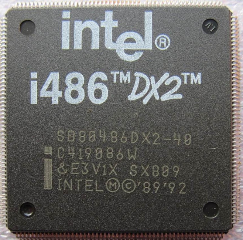
Intel 486DX2-40
The P24 DX2 486 processors introduced the CPU clock multiplier, doubling the system bus speed, while the system bus frequency itself was configurable via motherboard jumpers or DIP switches. Initially including 20, 25 and 33MHz options (later augmented by 40 and 50MHz models), users had a path to overclocking that didn't require soldering and replacing the clock crystal oscillator.
Alternatively, you could get the performance of a $799 DX2-66 by purchasing the more modestly priced 486DX2-40 for $400 and raising its default bus speed from 20MHz to 33MHz.
Stability and VLB slot issues at bus speeds over 33MHz meant that overclocking headroom decreased as the base clock rose – to the extent that many Intel DX2-66s wouldn't overclock at all and the few that did were often limited to 80MHz (2 x 40MHz).
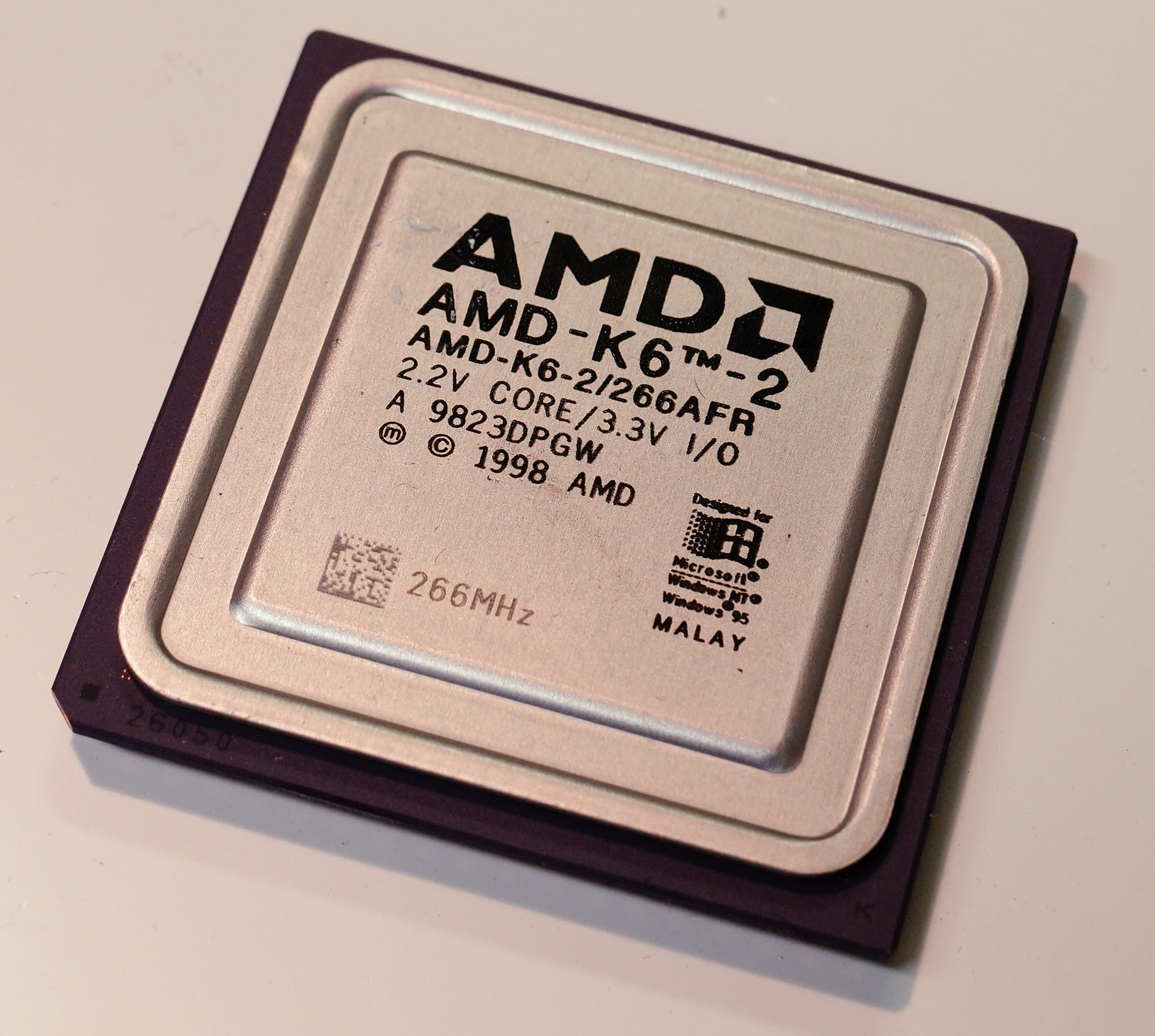
AMD K6-2 300 / 350
Though the K6-2 struggled against Intel's Pentium II and III in raw performance, it was extremely popular among enthusiasts looking to build affordable PCs. The addition of 3DNow! instructions gave it a slight edge in multimedia and gaming workloads that could leverage SIMD.
Enthusiasts with Super Socket 7 motherboards often pushed the 300 and 350MHz models to 400MHz and beyond. While not revolutionary in terms of clock headroom, the K6-2's wide availability, low cost, and tweakability made it a memorable part of the overclocking culture of the late 1990s.
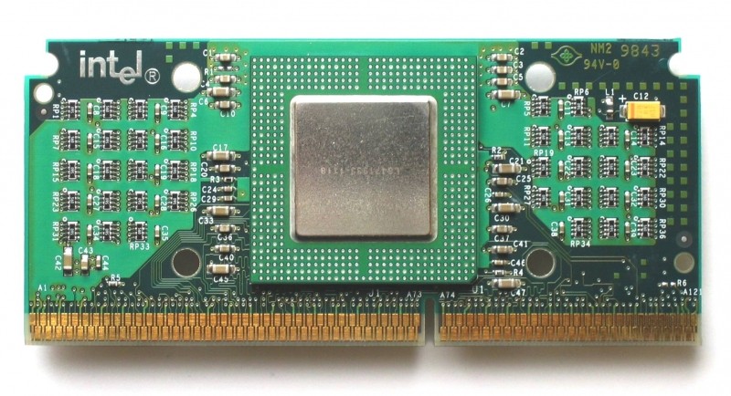
Intel Celeron 300A
Think legendary. The Celeron 300A was largely responsible for reigniting mainstream processor overclocking in the late 90's through the ease that it could be accomplished. A 50% overclock to 450MHz was as simple as changing the bus speed from its nominal 66MHz to 100MHz. Although some boards topped out at 83.3MHz limiting the OC to 375MHz, motherboards that supported 103MHz FSB could yield 464MHz.
A better chip with a voltage bump could run at the 112MHz FSB setting to produce 504MHz. Remarkably, the 300A could generally reach 450MHz without any additional voltage requirement over the nominal 2.0 volts. The chip's performance was also aided by having an on-die L2 cache and with a price of $149 it was particularly accessible to system builders.
Also worth mentioning, Intel's Celeron 366 (Mendocino) famously hit 550MHz with a good cooler and a 100MHz FSB. Right after the 300A, it was part of the golden age of overclocking on the cheap.
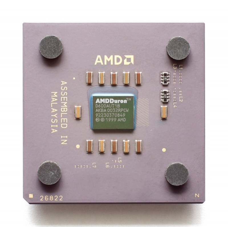
AMD Athlon 700 (Thunderbird) / Duron 600 (Spitfire)
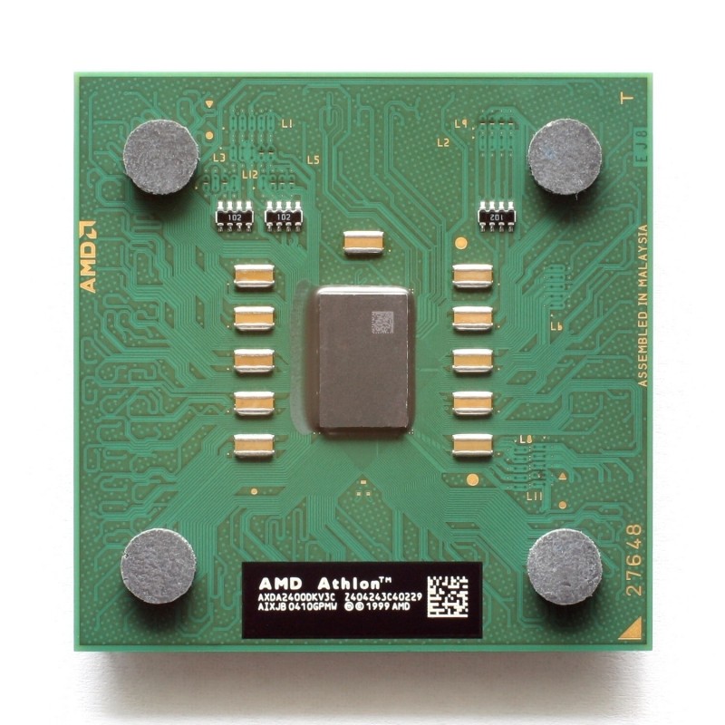
AMD's Thunderbird pencil mod was an overclocker's dream. AMD locked the voltage and multipliers of its K7 line in an effort to curtail the fraudulent remarking of processors to higher specifications. Overclockers quickly realized that the circuit bridges built into the silicon package held the key to unlocking performance.
Initially, a combination of connecting bridges in the L3, L4, and L6 blocks gave way to the bridging of L1 connections to unlock the multiplier. Bridging L7 connections to alter core voltage was also an option and the process could be as easy as using a soft lead pencil or conductive silver pen.
With AMD's EV6 system bus being sensitive to overclocking, multiplier overclocking provided results with the Duron leading the way thanks to its lower base core voltage (1.5v versus 1.7 /1.75v), which enabled higher relative overhead to the maximum 1.85v allowed.
For $112 and a little time, the Duron 600 easily approximated the performance of a processor many times its price.
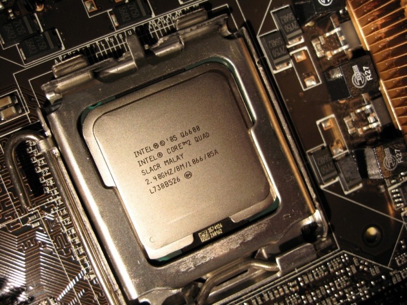
Intel Core 2 Quad Q6600
The Core 2 Quad Q6600 achieved an enviable record of longevity and performance value, becoming the de-facto choice for overclockers who wanted a budget quad-core CPU. Once the processor dropped in price from the initial $851 in January 2007, it quickly fell to $530 in May and further pricing realignment in July coincided with the arrival of the G0 revision. At $266, the 2.4GHz quad-core chip was priced identically to the new dual-core 3GHz E6850, a frequency that the earlier B3 revision Q6600 could comfortably eclipse.
The new G0 stepping offered slightly lower power consumption, which translated into the same improvement in overclocking ability, resulting in many users being able to sustain 3.4 to 3.6GHz fairly readily. The introduction of the affordable Intel P35 platform and further Q6600 price cutting through 2008 to $224 (April) and down to $183 (October) provided the opportunity for solid overclocking in the 50% range (9x multiplier x 400MHz FSB for 3.6GHz) on a moderate budget that remained very competitive long after many of its contemporaries had faded.
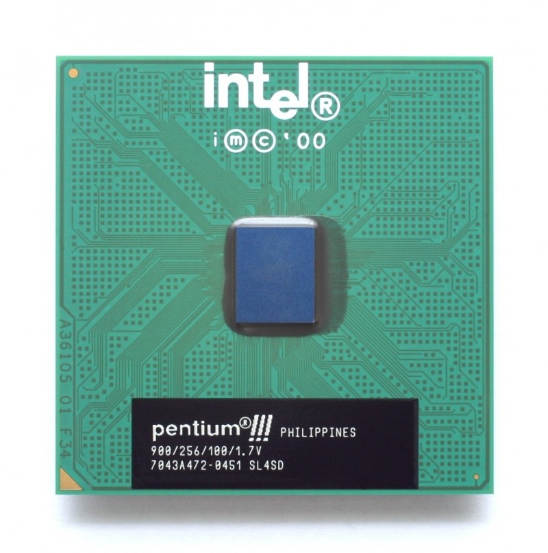
Intel Pentium III 500E
The Coppermine Pentium III 500E and 550E's overclockability lie in conservative binning, a low 100MHz Front Side Bus and the processor's integrated L2 cache. Budget pricing ($239) and the possibility of using older Slot 1 motherboards via Socket 370 to Slot 1 adapters enabled premium performance for a modest outlay.
The 500E could easily be run at 667MHz by selecting the motherboard's 133MHz FSB BIOS option or by using tape or lacquer to isolate the Slocket's A14 pin, while 750MHz (150 FSB) and higher were possible on better boards, producing performance equivalent to the $850 Pentium III 800.
However, there were some caveats to overclocking, including that motherboards needed to support AGP and PCI clock dividers (1:2 and 1:4 respectively) to maintain stability for attached components and fast PC133 RAM.
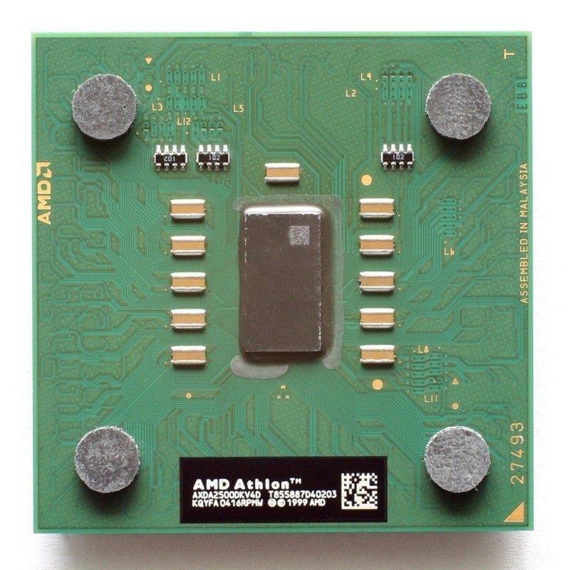
AMD Athlon XP-M 2500+ (Barton Mainstream 45W TDP)
In early 2004 it came to the attention of the overclocking community that the mobile Barton processors featured an unlocked clock multiplier in addition to being binned for low-voltage operation (1.45v compared with the desktop 1.65v). These factors often produced phenomenal overclocking headroom – something lacking in the desktop models.
When the chip's overclocking potential was publicized, such was the stampede that its price escalated over 30% from the $75 MSRP in a matter of weeks. With a solid nForce2 motherboard, decent cooling and a willingness to push the voltage to 1.8v and higher, a 30 to 40% overclock was often attainable. While the impressive speed bump couldn't bridge the performance gap to the new Athlon 64s, the Athlon XP-M 2500+ didn't cost $200 to $400 either.
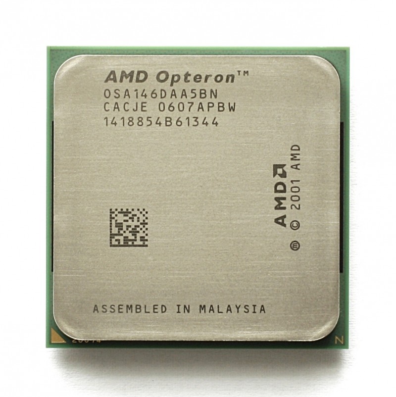
AMD Opteron 144 / 146 (K8 Venus)
Featuring the same silicon as AMD's San Diego-based Athlon 64 processors, the $125 and $183 Socket 939 Opterons enjoyed a significant pricing advantage over the similarly featured Athlon 64 3700+ at $329 and stacked up even better against the $1,000 FX-57.
Like all upwardly locked multiplier processors, the Opteron's ability was tied directly to the strength of the motherboard being used. Conservative binning of the Opteron server chips allied with a solid overclocking board such as those sporting the nForce4 chipset with HyperTransport frequencies approaching (and exceeding) 300MT/sec would lead to overclocks seldom seen with enterprise-class processors.
With all the Opteron models having roughly the same overclock ceiling, the lowest priced 144 sold out quickly in many markets.
Intel Core i7 2600K / Core i5 2500K
When Intel announced an upper clock multiplier limit and almost non-existent system bus overclocking for its upcoming Sandy Bridge compatible Cougar Point chipsets, it was widely touted as the end of overclocking on Intel platforms. The truth turned out to be that the 2500K and 2600K were premier overclockers requiring minimal effort in time and cooling for stable overclocks in the 30 to 50% range.
Such was the popularity of the 2600K that submissions from this processor accounted for around 28% of all CPU results to HWBot in 2011 and would exceed those of its successor, the 3770K, in 2012. A low cost of $216 plus solid cooling results when paired with either air or water made Intel's 2500K the de facto standard by which all other consumer CPUs were judged.
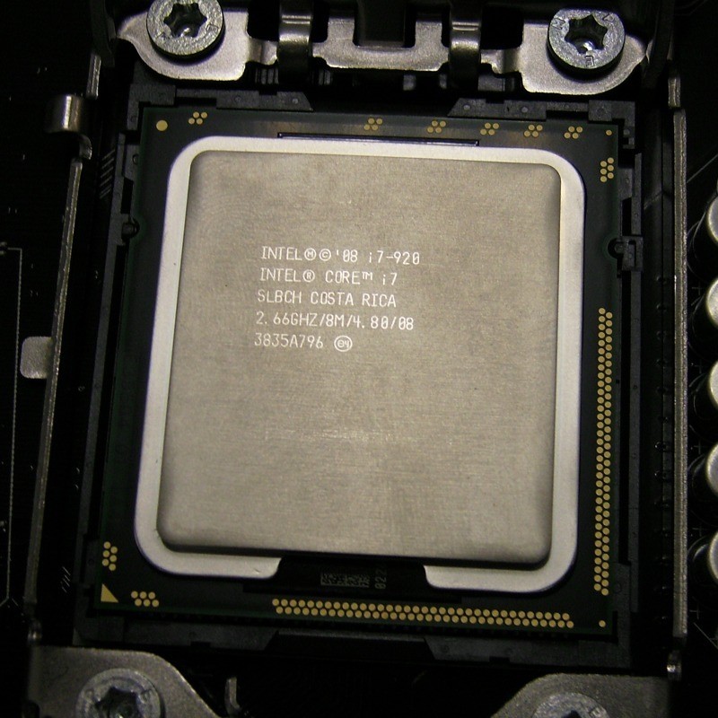
Intel Core i7 920
The new Nehalem architecture and X58 platform offered enough promise to coax many users from long-lived Core 2 LGA 775 systems. While the flagship i7 965 EE at $1,000 was cheaper than the Core 2 QX9770 by a third, it still represented little in the way of value compared to the i7 920.
Initial C0 revision Bloomfield CPUs earned a reputation for high voltage requirements past 3.6GHz, the following D0 often had the ability to maintain the nominal 1.26v up to 4GHz and an absolute overclock ceiling approaching 4.5GHz for those tempted to turn the voltage closer to 1.5v.
Such was (and is) the 920's popularity that it represents over a third of HWBot's overclocking submissions for 64 LGA 1366 processors.
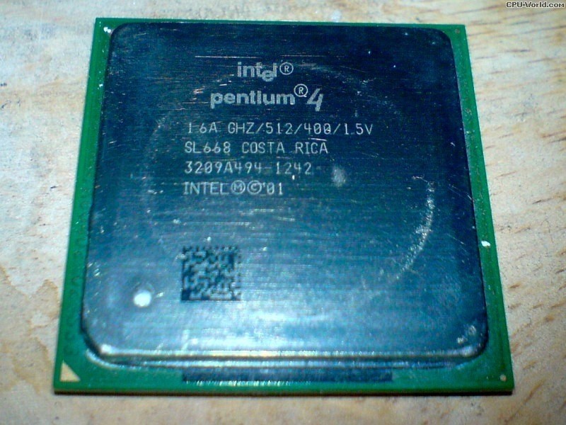
Intel Pentium 4 1.6A / Celeron 2.0 (Northwood)
The arrival of the Northwood core was a welcomed sight after the disappointing Williamette, whose voltage and resulting heat stifled serious overclocking for the mainstream. While the higher-clocked P4s offered little if any value against the Athlon XP, the 1.6A at $125 turned a performance deficit into a win with its low base FSB of 100MHz which could easily be increased to 150 for a 2.4GHz clock speed.
The Celeron's overclock was higher still thanks to a 20x multiplier, although performance was heavily constrained by the meager 128KB L2 cache. Those seeking higher overclocks would need to push the core voltage past 1.6v either through BIOS settings or the wire mod (connecting CPU pins to raise Vcore limits), the latter being largely responsible for the phenomena of S.N.D.S. (Sudden Northwood Death Syndrome), more commonly known as electromigration.
This factor and the 1.6A cannibalizing Intel's own higher priced models are seen as the motivation for the company to cease sales of the 1.6A barely six months after its introduction in January 2002.
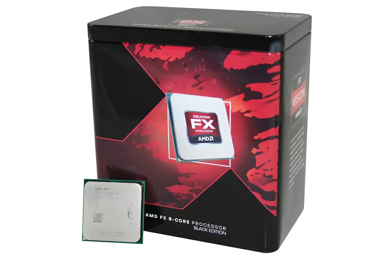
AMD FX-8350 (Vishera)
The FX-8350 was a polarizing chip. Based on AMD's Piledriver architecture, it was marketed as an 8-core processor, though in reality it had four integer modules with dual-core capabilities. While its single-threaded performance lagged behind Intel's offerings, the FX-8350 became an overclocking favorite due to its unlocked multiplier and incredible thermal headroom.
Many users pushed it past 5GHz with good aftermarket cooling, and it became a cult classic in the enthusiast scene, especially in budget gaming rigs and benchmark competitions.
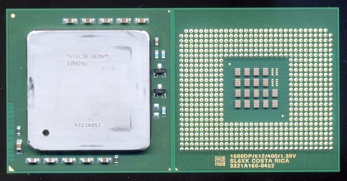
Intel Xeon LV 1.6 D1 (Prestonia)
Overclocking is most often associated with gaming systems, but dual-processor overclocking has maintained a solid following for over a decade. Long before the QX9775 and Intel's Skulltrail board became the watchwords for performance excess, many enthusiasts sought the budget Xeon LV 1.6.
The Prestonia core was basically the Pentium 4 Northwood with SMP (symmetric multiprocessing) and HyperThreading added as standard features. With the sub-$200 1.6GHz Xeon drawing a frugal 1.274v, overclockers generally couldn't take advantage of voltage headroom as most boards were voltage-locked. However, simply raising the FSB would net 2.6GHz.
For the more adventurous, three hard mods could yield a 100% overclock (or more!): the U-Wire mod which involved bridging two (1.5v) or three (1.6v) sets of socket pins, the BSEL mod to isolate or break CPU pins and raise the FSB limit to 200MHz, and the vDIMM mod to raise RAM voltage.
Those willing to push the limits of the technology could be rewarded with a 3.2GHz dual processor performance king for around $700 (CPUs, coolers, board, and RAM).
AMD Athlon XP 1700+ (Thoroughbred-B)
The initial Thoroughbred-A was little more than a die shrink of the previous Palomino and was somewhat disappointing as a final product. The June 2002 introduction of AMD's Thoroughbred-B was more tuned for the 130nm process and resulted in higher core frequencies along with being more efficient as the 'B' revision demonstrated a remarkable overclock ability with minimal if any voltage increases.
Allied with a strong nForce2 chipset motherboard, the $60 XP 1700+ was fully capable of near 2GHz core speed at its default voltage. With an nF2 board capable of pushing the system bus past 200MHz, it was possible to sustain a 40% overclock with a modest 1.7v, eclipsing the performance of AMD's $397 Athlon XP 2800+ flagship and putting Intel's Pentium 4 on notice.
Intel Pentium D 820 / D 805
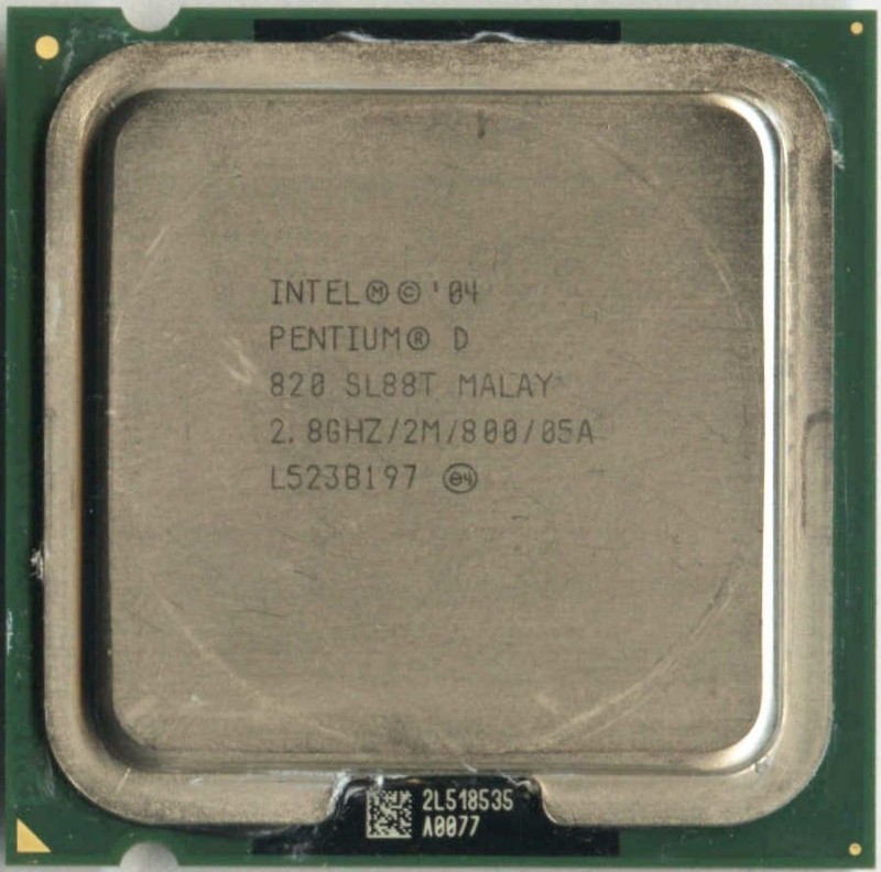
The Pentium D 820 was something of an anomaly with two single cores on an MCM package for much cheaper than the cheapest dual-core AMD Athlon 64 X2 at $241 and even undercut the single core Athlon 64 3500+ by $30. The Pentium D 820 offered modest performance in no way challenging the Athlon dual, but some considerable overclocking headroom with judicious voltage and a good air or water-cooling system.
The arrival of Intel's $129 D 805 further endeared the hot Netburst processor to the budget overclocker. A reduction in nominal system bus speed from 200MHz to 133 was offset by the D 805's 20x clock multiplier, resulting in no reduction in overclocking fun. For those of modest means, a D 805 paired with a solid 945P board and value-orientated RAM held the promise of performance that was the province of a $500 processor-dictated build.
Intel Pentium Dual Core E2140 / E2160
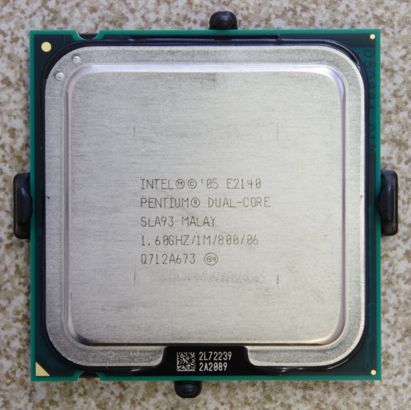
Intel's E2000 series effectively signaled the end of both the last surviving NetBurst Pentium D and AMD's dominance in the budget market. Intel would halve the L2 cache of the E4000 series and further hobble performance with a 200MHz (800 FSB) system bus. What Intel didn't do was remove the Conroe processor's ability to overclock.
You could hit a 50% overclock with default voltages and the stock cooler by simply raising the bus speed to 300MHz on either an affordable Intel-based P965/P35 board or one with an Nvidia 650i SLI chipset which allowed greater options with cheaper RAM thanks to its non-reliance on memory dividers.
An aftermarket air cooler, voltage adjustment and some luck in the silicon lottery could see the processors at or near a 100% overclock, delivering performance around the level of the E6700 for a fraction of the cost.
Intel Core i5 750 (Lynnfield)
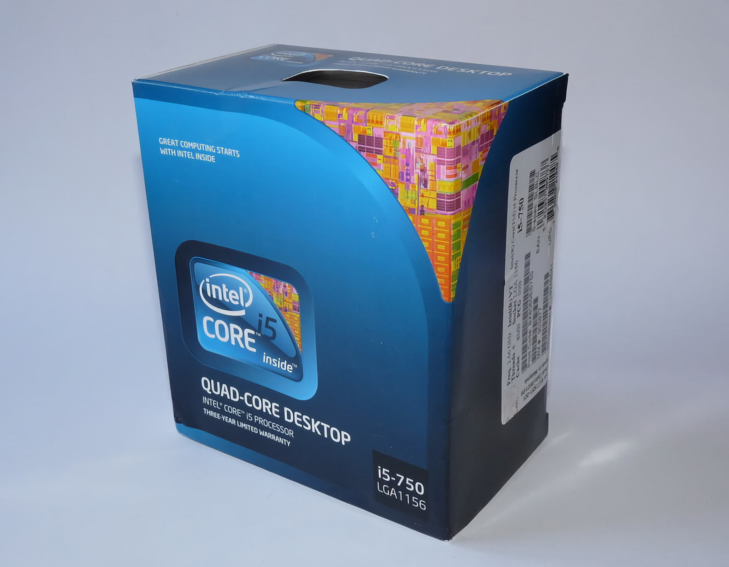
The Core i5 750 was Intel's first mainstream quad-core processor without Hyper-Threading, based on the Nehalem-derived Lynnfield architecture. It featured an integrated memory controller and a DMI link for PCIe directly from the CPU, improving latency and efficiency.
Though it lacked an unlocked multiplier, its base clock (BCLK) was highly tweakable, allowing enthusiasts to reach nearly 4GHz with good cooling. As the first true successor to Core 2 Quad on the LGA1156 platform, it became a gateway chip into the Nehalem era and remained viable for years with overclocking.
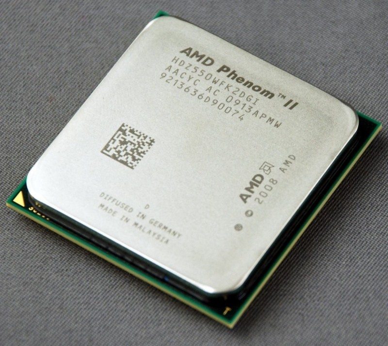
AMD Phenom II X2 550 Black Edition (Callisto) / X4 955 Black Edition (Deneb)
The release of AMD's revised K10.5 architecture during the early months of 2009 marked a resurgence of the company's strong value proposition. The emergence of the Black Edition processors also added the welcome addition of the unlocked multiplier to facilitate overclocking.
While the eventual clock speed increases weren't excessive by historical standards, they did go hand in hand with actual performance gains which comfortably lifted them out of the Core 2 Quad shadow. At $100, the 550 Black Edition represented a superlative value if the two disabled cores could be unlocked (the unlocking of the fourth core would be a major selling point for the X3 720 BE), while the outright performance of the $245 955 BE ensured that only Intel's more expensive X58 platform exceeded its potential.
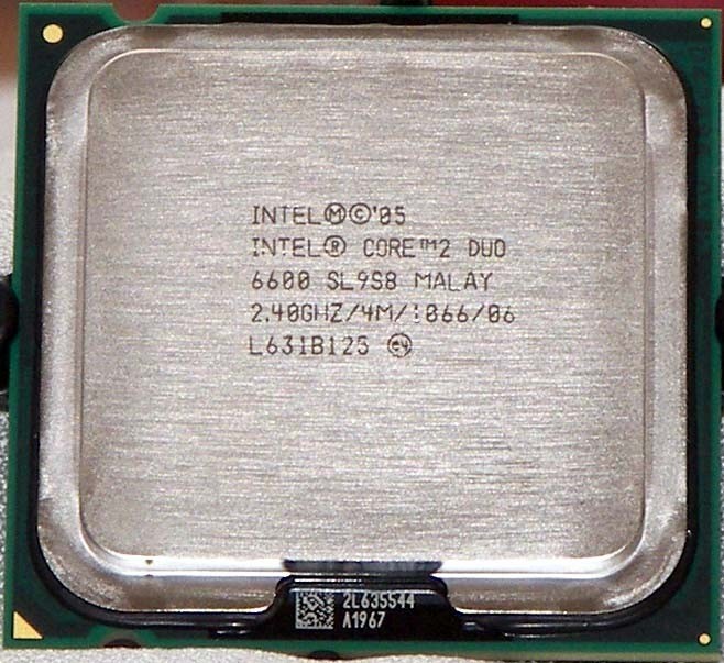
Intel Core 2 Duo E6600 (Conroe)
When Intel's Conroe architecture arrived in July 2006, most of the attention was focused on the unlocked multiplier X6800, but it was the cheapest fully enabled (4MB L2 cache) chip that stole the show. For $316, the chip cost a full $200 less than the next step up in performance (the E6700) and already provided results that rivaled AMD's top Athlon 64s.
With stock cooling and default voltages, you could generally rely on the E6600 to hit 2.7 to 3GHz. If you had an aftermarket cooler, motherboard stability was often the limiting factor as system bus speeds flew past 400MHz and edged towards 450. Such was the overclocking potential that the $999 X6800 and $799 Athlon 64 FX-62 looked positively ludicrous when comparing price and performance with the E6600.
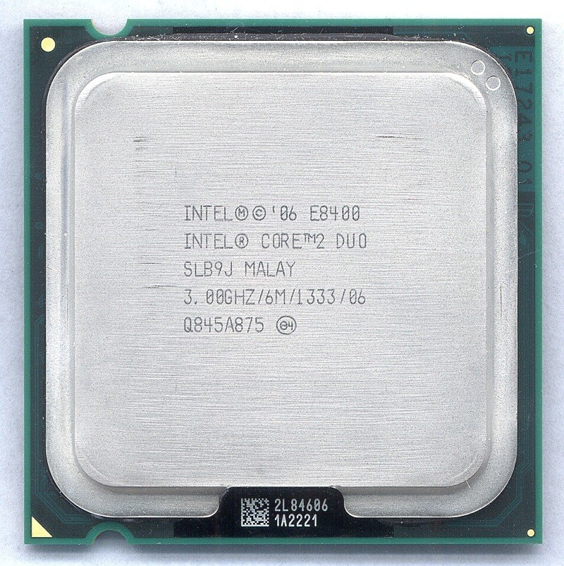
Intel Core 2 Duo E8400 E0 (Wolfdale-6M)
The initial January 2008 C0 revision Wolfdale-based E8400 had immediately ensconced itself as an affordable performance overclocking processor. Five months later, the E0 revision brought a much refined voltage requirement. While some C0-step E8400s were capable performers at the 4GHz level, more often than not, the same frequency could be achieved with stock voltage, settings, and cooler with the new revision.
By the time the E0 arrived, pricing had fallen to $149 for the OEM package with a range of very capable P45 and X48 boards able to maintain bus speeds in the vicinity of 500MHz (2000MHz FSB). The continued stability of these 4+GHz systems many years later is a testament to the quality of both the architecture and the chipsets.
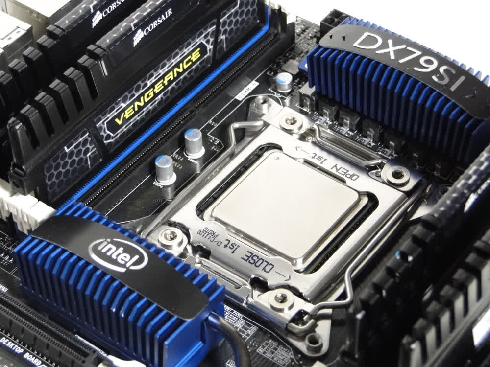
Intel Core i7 3930K (Sandy Bridge-E)
The Core i7 3930K was Intel's answer to high-end enthusiasts and prosumers in the early 2010s. Featuring 6 cores and 12 threads on the Sandy Bridge-E platform, the chip ran on the LGA 2011 socket and required the X79 chipset.
Thanks to its unlocked multiplier and improved thermals over earlier hex-core offerings, the 3930K routinely achieved overclocks above 4.5GHz with adequate cooling. Paired with quad-channel memory and strong motherboard VRMs, it became a go-to chip for power users, gamers, and video editors, maintaining relevance well into the Skylake era.
Image source: PCPer
Intel Core i7 4790K (Devil's Canyon)
Devil's Canyon was Intel's response to criticisms of Haswell's poor thermals. With improved thermal interface material (TIM) and refined power delivery, the 4790K was the highest-clocked stock CPU Intel had ever released at the time.
Overclockers consistently reached between 4.7GHz and 5.0GHz on air or AIO water cooling setups. Its exceptional single-threaded performance and consistent stability made it a mainstay in gaming builds for years, with many systems built on Z97 platforms continuing to deliver long after newer generations had arrived.
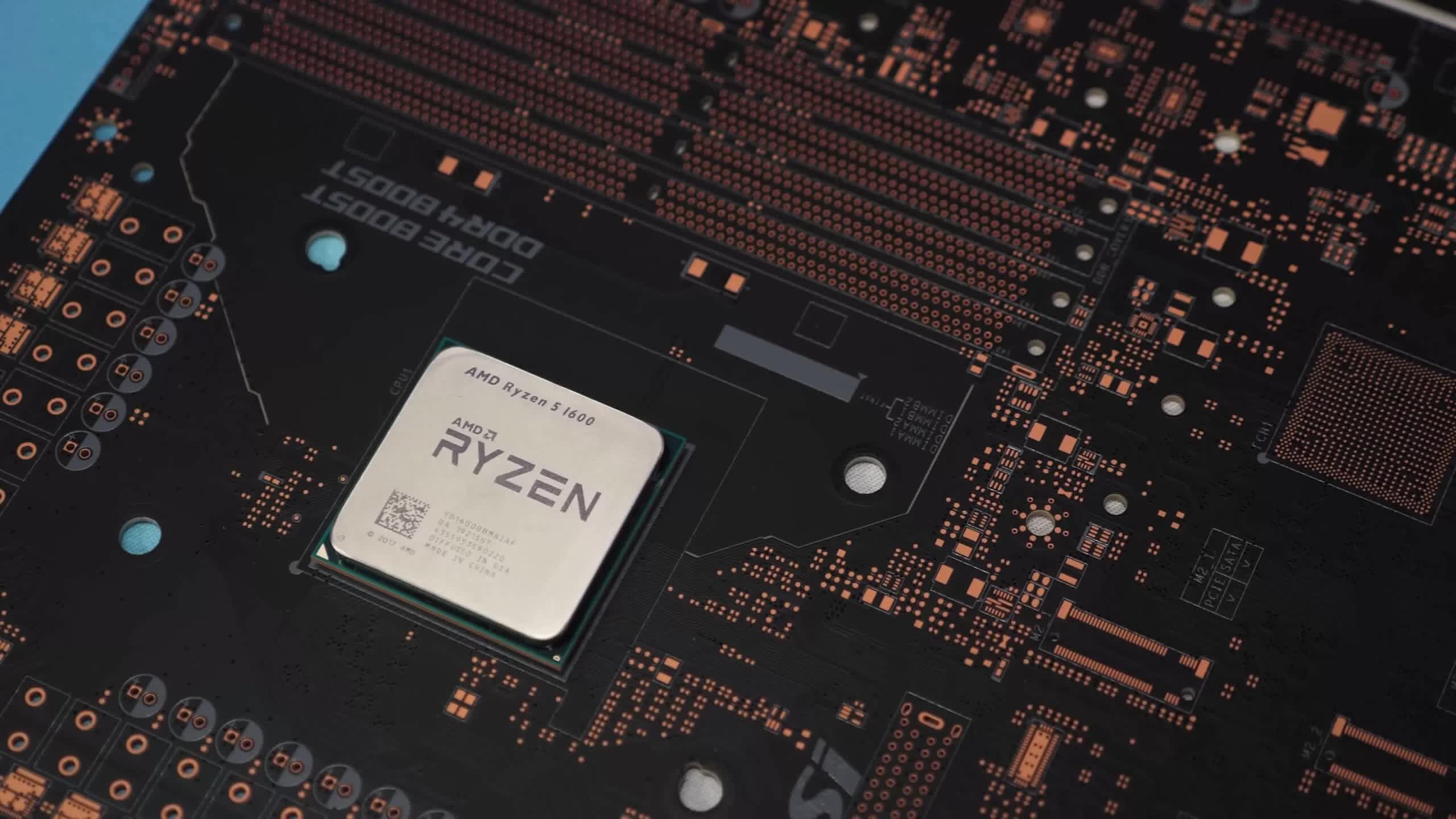
AMD Ryzen 5 1600 AF
Initially thought to be a re-release of the original Ryzen 5 1600, the 1600 AF turned out to be a hidden gem. Manufactured on the newer 12nm Zen+ process rather than the original 14nm, the chip effectively performed like a Ryzen 5 2600 while retaining the original name and lower price tag.
Thanks to improved thermal efficiency and better memory support, overclockers routinely pushed it to nearly 4.2GHz. The 1600 AF became an unbeatable value proposition in 2020, offering six cores and twelve threads at around $85 and dominating the budget enthusiast scene.
More tech enthusiast content at TechSpot:
Read about the history of the microprocessor, the rise, fall and revival of AMD, or the best CPUs you can buy right now. For lighter reading... check out our top 10 tech pranks and computer tips & tricks you should know about.


