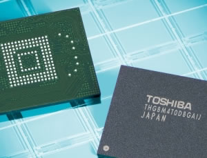
Toshiba has introduced new flash memory chips that offer more performance and storage capacity in less space than existing parts. The company's new 24nm e-MMC chips feature toggle-mode double data rate (DDR) NAND flash memory, which boosts random access and sequential performance over single data rate NAND. All the while, they offer plenty of storage capacity for today's smartphones, tablets, e-book readers, digital cameras, printers, and more.
The JEDEC e-MMC v4.41-compliant parts cram up to 128GB of NAND (16 64Gb/8GB chips) alongside an e-MMC controller in a single package – a feat that Toshiba claims to be the first to achieve. Featuring the world's smallest geometry e-MMC, the company's new components utilize advanced chip thinning and layering technologies to produce parts measuring only 30 micrometers thick (0.0001 inches – thinner than the average human hair).
"The utilization of our new toggle-mode DDR NAND die at 64Gbit density is key to enabling our e-MMC to support the higher performance, and smaller, thinner packages that customers desire," said Scott Beekman, Toshiba America's senior business developer manager of mobile communications memory . "For example, our 128GB e-MMC can now be supported in a smaller 14 x 18 package, which many space conscious applications can support."
We've included Toshiba's list of key features at the end of the post. Samples of 8GB, 16GB, 32GB and 64GB packages are already shipping with mass production set for the third quarter. Meanwhile, 2GB, 4GB and 128GB densities will begin sampling later this year with mass production scheduled for the fourth quarter of 2011 or first quarter of 2012. The company hasn't said precisely who plans to purchase the chips or what devices they'll appear in.
- Faster performance using toggle-mode DDR NAND.
- The JEDEC e-MMC V4.41 compliant interface handles essential functions, including writing block management, error correction and wear leveling. It simplifies system development, allowing manufacturers to minimize development costs and speed up time to market for new and upgraded products.
- A wide product line-up supports capacities from 2GB to 128GB.
- The 24nm 64Gbit die enables smaller e-MMC packages.
- The new chips support the advanced partitioning and security of e - MMC V4.41. Multiple storage areas can be configured, including several enhanced memory areas for system files or code, and a multi-level cell (MLC) area for data storage.