Intel is developing discrete GPUs for gamers, professionals, and servers, and they're all slated for release this year or coming in 2021. Intel's cards will either be the long-awaited saviors of a stagnant market, or they'll underperform and flop miserably (no pressure, Intel PR person reading this). Personally, I'm happy either way: we get good GPUs, or we get some good stuff to make fun of.
This is our second round of investigation into Xe, as quite a bit has transpired in the last few months. To quickly recap here's a timeline of the major announcements Intel has made since the moment they went public with Xe's development:
- November 8, 2017: Raja Koduri quits his job running AMD's GPU department and joins Intel, becoming their Senior VP of core and visual computing. His first act is to hire a half-dozen old buddies from within AMD's ranks.
- June 12, 2018: Then-CEO Brain Krzanich reveals to Intel's investors that they've been designing an Arctic Sound discrete GPU architecture for years, and they plan on releasing it in 2020.
- January 8, 2019: Senior VP of client computing Gregory Bryant confirms at CES that Intel's first round of GPUs will arrive on the 10nm node.
- May 1, 2019: Jim Jeffers, senior principle engineer and director of the rendering and visualization team, announces Xe's ray tracing capacity at FMX19.
- November 17, 2019: Raja Koduri reveals Xe will come in three flavors, high-performance, low-power, and high-performance compute. He says the first GPU in the latter category will be Ponte Vecchio, coming in 2021 on the 7nm node.
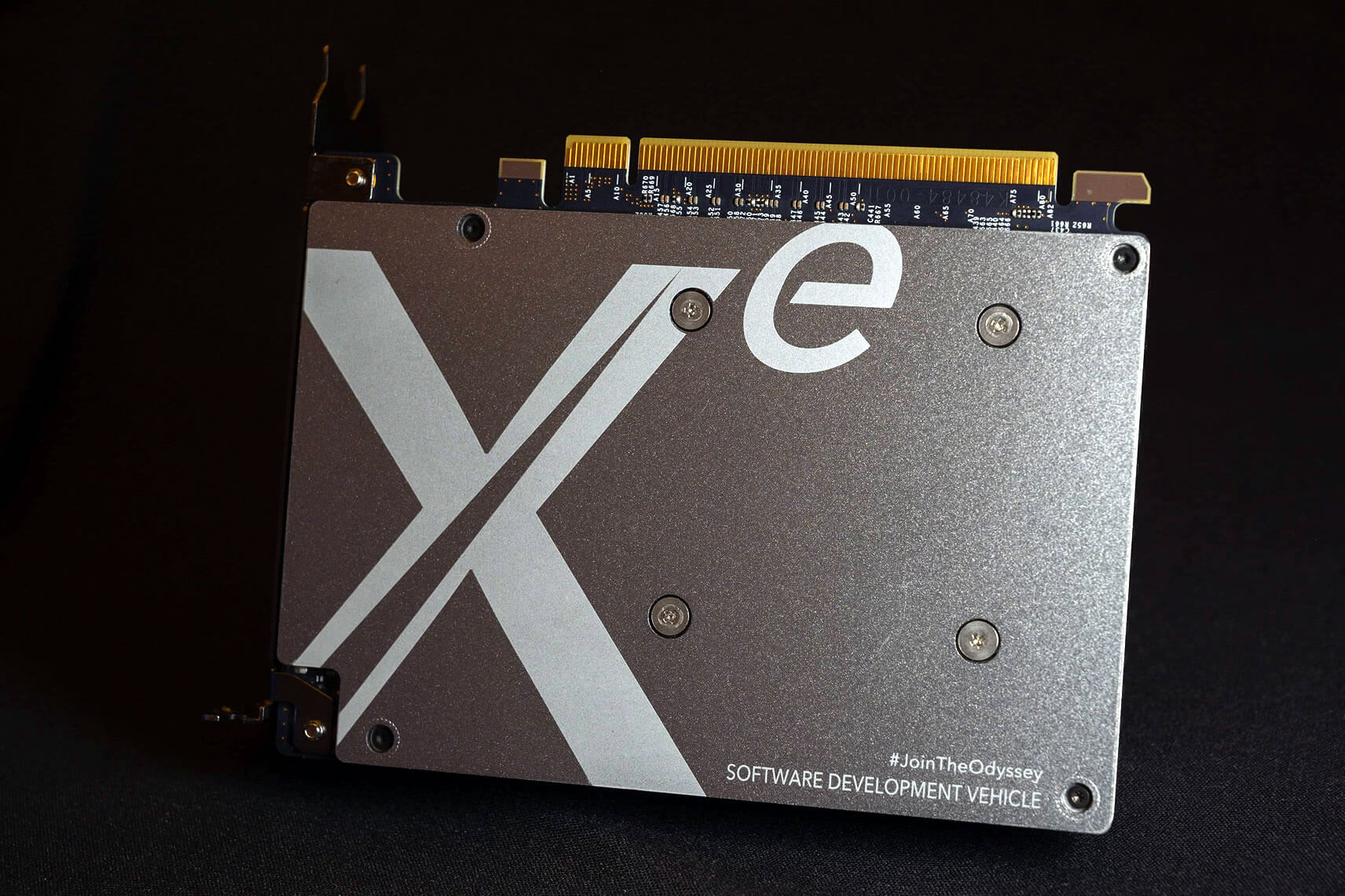
- January 9, 2019: The first images of the Discrete Graphics One Software Development Vehicle (DG1 SDV) are published, showing a small RGB-infused card helping developers optimize their software for the Xe architecture.
And soon...
- March 17, 2020: Senior developer relations engineer Antoine Cohade will "provide a detailed tour of the hardware architecture" and the "performance implications" of Xe at GDC.
The official narrative spins a tale of Intel hard at work building mysterious GPUs infused with many desirable features; better nodes, ray tracing, new packaging techniques. But you and I both know it's not the gimmicks that make a GPU, but the horsepower and cash involved. That's what this article is about.
Architecture
A good architecture starts with one brick, and so do GPUs... except for Intel's. AMD and Nvidia's cores perform one operation per clock, but Intel's execution units (EUs) perform eight. Despite the technical inaccuracies, however, we're going to describe one EU as being equivalent to eight cores for comparison purposes.
Apart from Intel's need to build with eight bricks at a time, their construction techniques are straightforward. They can throw a few bricks together and make a wall. A few walls and you get a room, chuck a couple of those together and you can make an apartment.
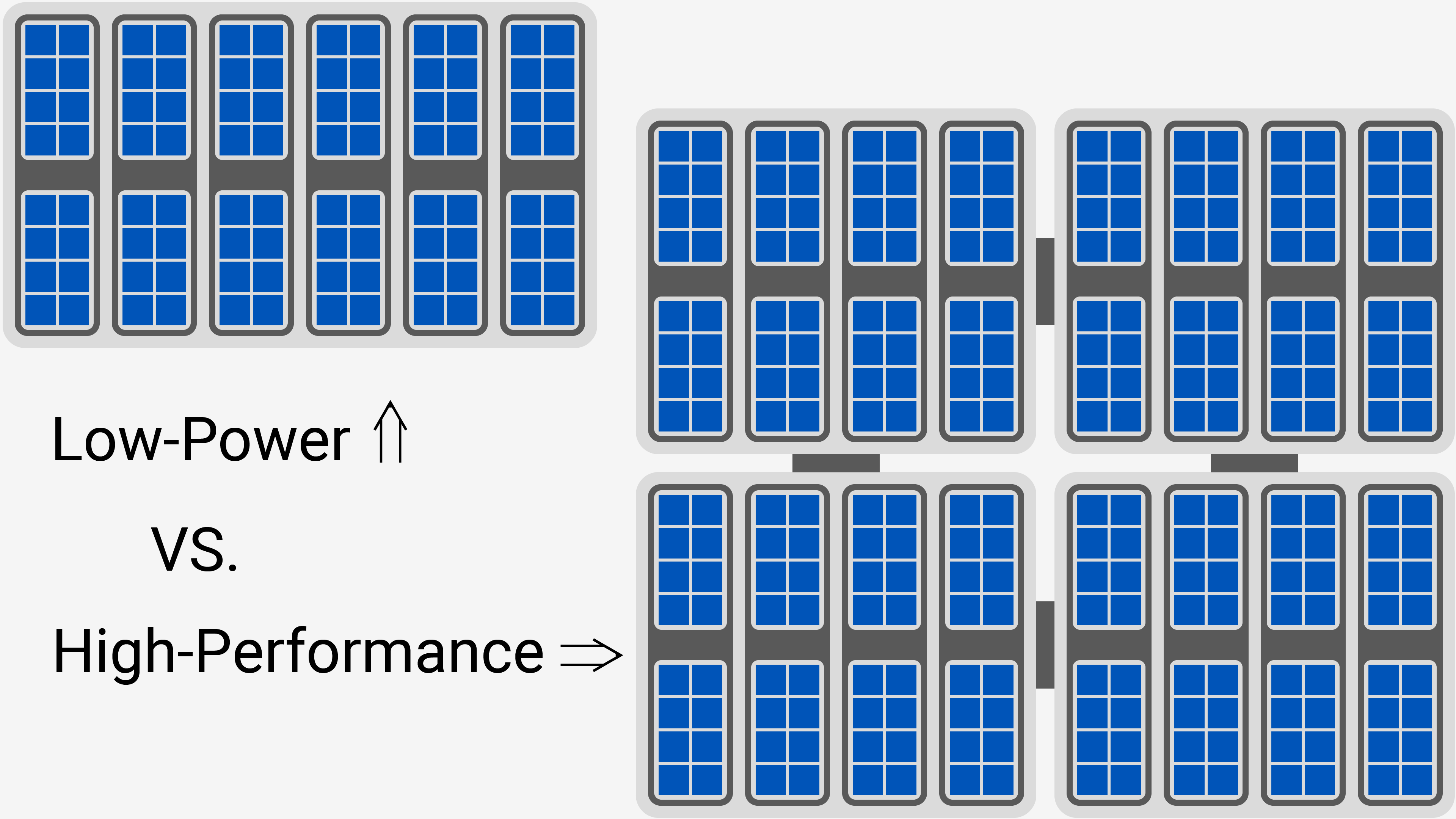
Skipping the intermediary steps, Xe's largest self-contained unit (the apartment) is called a slice and each one contains 512 or 768 cores, for high-performance and low-power slices, respectively. One apartment is all you need, so the low-power cards use just one slice. But if you don't want to settle there, Intel is building skyscraper-style enthusiast GPUs made of many slices.
That's all you need to know about the Xe architecture to grasp what's going on, but if you can speak some technobabble and like numbers, don't skip this next bit.
In Gen11, Intel's integrated GPUs had one slice made of eight sub-slices, which in turn had eight execution units each. They've rejigged this slightly for Gen12 (Xe's first-gen) and are including compute units (CUs) along with changes to the render backend.
In September, code accidentally uploaded to GitHub leaked the configurations of DG1, Ponte Vecchio, and one DG2 variant. This leak is reliable, as its counter-intuitive prediction that Ponte Vecchio will have two slices was proven correct. Its prediction that DG1 will have six sub-slices per slice and thus 96 EUs was also more or less confirmed by an EEC filing that gives the same number.
The leak reveals that in all their Gen12 models, Intel has 16 EUs per sub-slice, and in Ponte Vecchio specifically, four sub-slices per slice. Koduri later revealed that Ponte Vecchio has two slices and sixteen CUs.
That's enough information to say that Ponte Vecchio probably works like this: eight EUs are combined into a CU (64 cores), which are paired into a sub-slice (128 cores/16 EUs), four of which make one slice (512 cores/64 EUs). With two slices that means that Ponte Vecchio has 128 EUs, 1024 cores. Note, the two-slice configuration may be just for prototypes.
Ponte Vecchio's basic slice configuration is expected to be used across high-performance and low-power models as well.
DG2: High-Performance
The high-performance microarchitecture, codenamed Discrete Graphics Two (DG2), envelops the mid-range and enthusiast GPU markets. It's these cards that'll have the ray tracing and RGB bling, but what's most exciting is the potential for Intel to challenge Nvidia's stranglehold on the premium $600+ range.
"Xe HP ... would easily be the largest silicon designed in India and amongst the largest anywhere." - Raja Koduri
Last July, Intel accidentally published a driver (thanks!) that contained three DG2 codenames, iDG2HP128, iDG2HP256, and iDG2HP512. Making the reasonable assumption that the three digits at the end indicate the card's number of EUs, then they'll have 1024, 2048 and 4096 cores, respectively. That's two, four and eight slices.
Not long after, however, we saw solid evidence of a three-slice GPU with 1536 cores being developed as well. Given it would be illogical for Intel to develop a fourth card spec'd so similarly to existing models, it's safe to assume this is an iDG2HP256 with one slice disabled. This supports widespread suspicions that Intel is taking the three fundamental models and disabling one or more slices to add fourth, fifth, sixth or even seventh models to their line-up.
| # of Slices | 1 | 2 | 3 | 4 | 5 | 6 | 7 | 8 |
| Core Count | 768* | 1024 | 1536 | 2048 | 2560 | 3072 | 3584 | 4096 |
| Codename | iDG1LPDEV | iDG2HP128 | iDG2HP256 | iDG2HP512 |
DG2 will also be more than just gaming GPUs. They won't be able to handle scientific workloads like Ponte Vecchio, but if they're good value on release, they could certainly be remarketed with professional drivers as video editing or 3D modeling hardware, like Nvidia's Quadro cards.
DG1: Low-Power
The low-power segment is defined as just that, 5W through to 50W. 5W to 20W for integrated GPUs, and 20W to 50W for discrete ones.
Intel has already introduced us to the first member of the LP family. The DG1 SDV was prominently displayed at CES 2020, running Destiny 2 and Warframe with RGB and all. But it's only dressing up as a gaming card. The DG1 SDV is a developer-only edition designed to help out with transitioning software and drivers to the Xe platform.
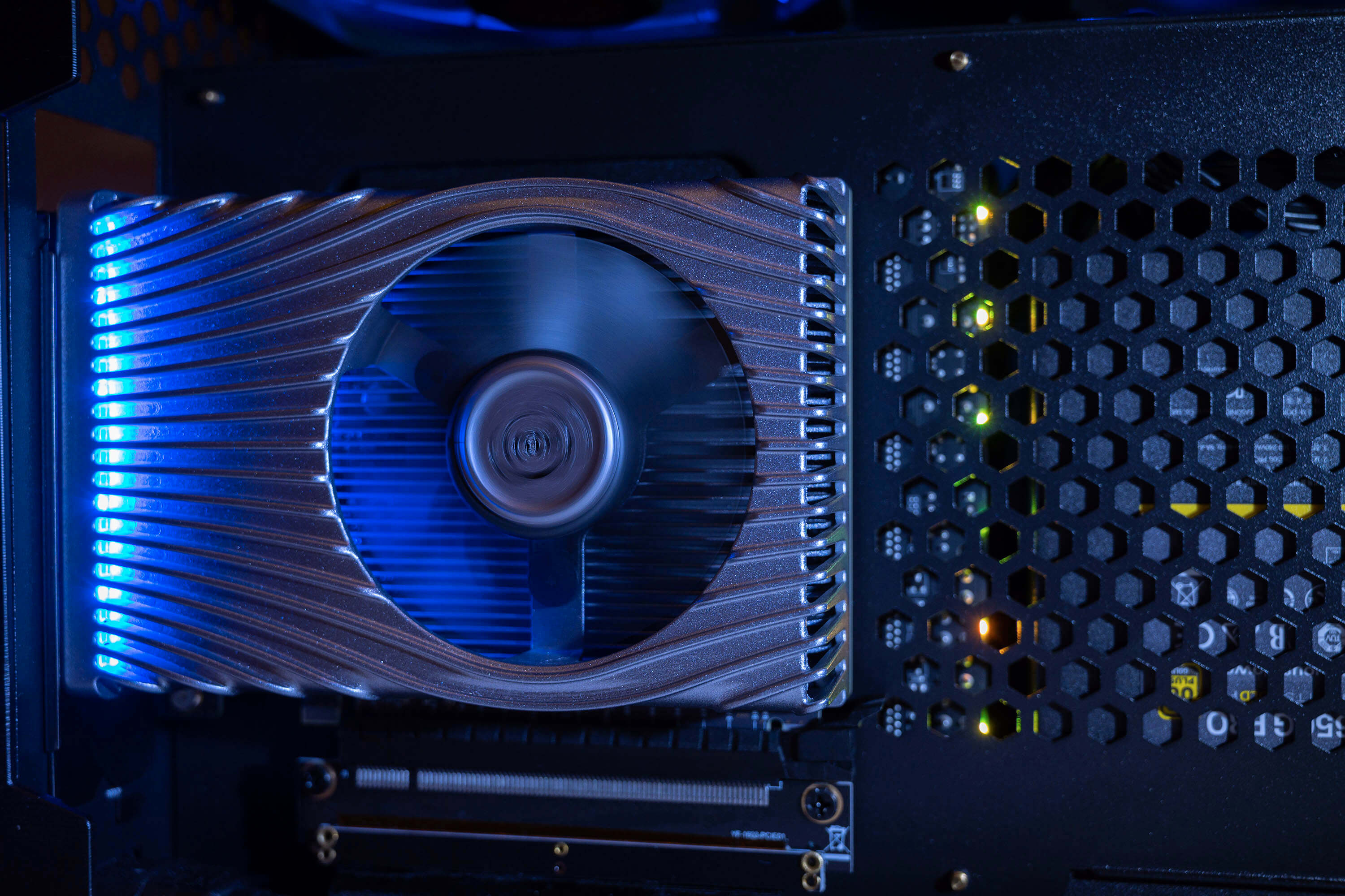
However, that doesn't mean you won't eventually be able to buy something fairly similar - Intel has already shown it running in a laptop.
Integrated forms of the LP GPU are reported to have between 64 and 768 cores, while discrete LP GPUs exclusively wield the full 768 cores. That's a comparable number of cores to AMD's best integrated hardware, and Nvidia's lowest-end discrete GPUs. But where Xe LP might outshine them is in clock speeds.
A leaked Geekbench run of a Rocket Lake mobile processor has shown an integrated 768 core LP GPU running at 1.5 GHz, netting it 2.3 TFLOPs. That's the same amount of performance as a GTX 1650. Even assuming the worst, that the 1.5 GHz uses the full 20W TDP and Intel won't be able to push speeds even 1 MHz higher before release, that's impressive.
Just imagine how efficient this processor must be. The GTX 1650 has slightly fewer TFLOPs and has a 75W TDP: almost four times as much. An LP GPU pushed to 50W will boost clock speeds higher and could enter the same performance bracket as a GTX 1660.
But the good stuff doesn't stop there. Updates to the Linux kernel show Intel is planning a way to run integrated and discrete graphics concurrently and potentially in conjunction. If this pans out, the full power of an iGPU could be paired with the discrete GPU's power to create a 1536 core combo GPU that is space-efficient and cost-effective. It's an excellent way to squeeze more performance out of the same silicon.
Ponte Vecchio: Data Compute
When I said in the introduction that only the raw horsepower of a GPU mattered, I lied intro clickbait confirmed. That's not the case for any data center GPU, and Ponte Vecchio in particular. Ponte Vecchio is all about the tricks and techniques that maximize efficiency.
Fun Fact:
Koduri named Ponte Vecchio after the bridge in Florence because he likes the gelato there.
Ponte Vecchio was created specifically with the Aurora supercomputer in mind, which should give you an indication of the type of workloads it will be optimized for.
If it didn't give you an indication, then I'll spell it out: double precision. It's basically the first thing on the list for every data center GPU, and Koduri spent a lot of his time discussing it during the reveal. Unfortunately, however, the only number he would put to it is Ponte Vecchio's per EU theoretical FP64 performance, which is ~40x that of Gen11's.
Doing some back of a napkin math, that's about 20 TFLOPs at FP64 per 1024 core card. Don't take that as gospel though, because there aren't enough significant figures in the calculation to yield meaningful results.
Second to high precision workloads, is, naturally, ultra-low precision work. Ponte Vecchio supports INT8, BF16, and the usual FP8 and FP16 for AI neural network processing. Each EU is outfitted with a matrix engine (like an Nvidia Tensor core) that is 32x faster than a standard EU for matrix processing.
However, none of that is particularly novel. Ponte Vecchio's true strength is in its memory subsystem, which lets the GPU tackle problems in new ways.
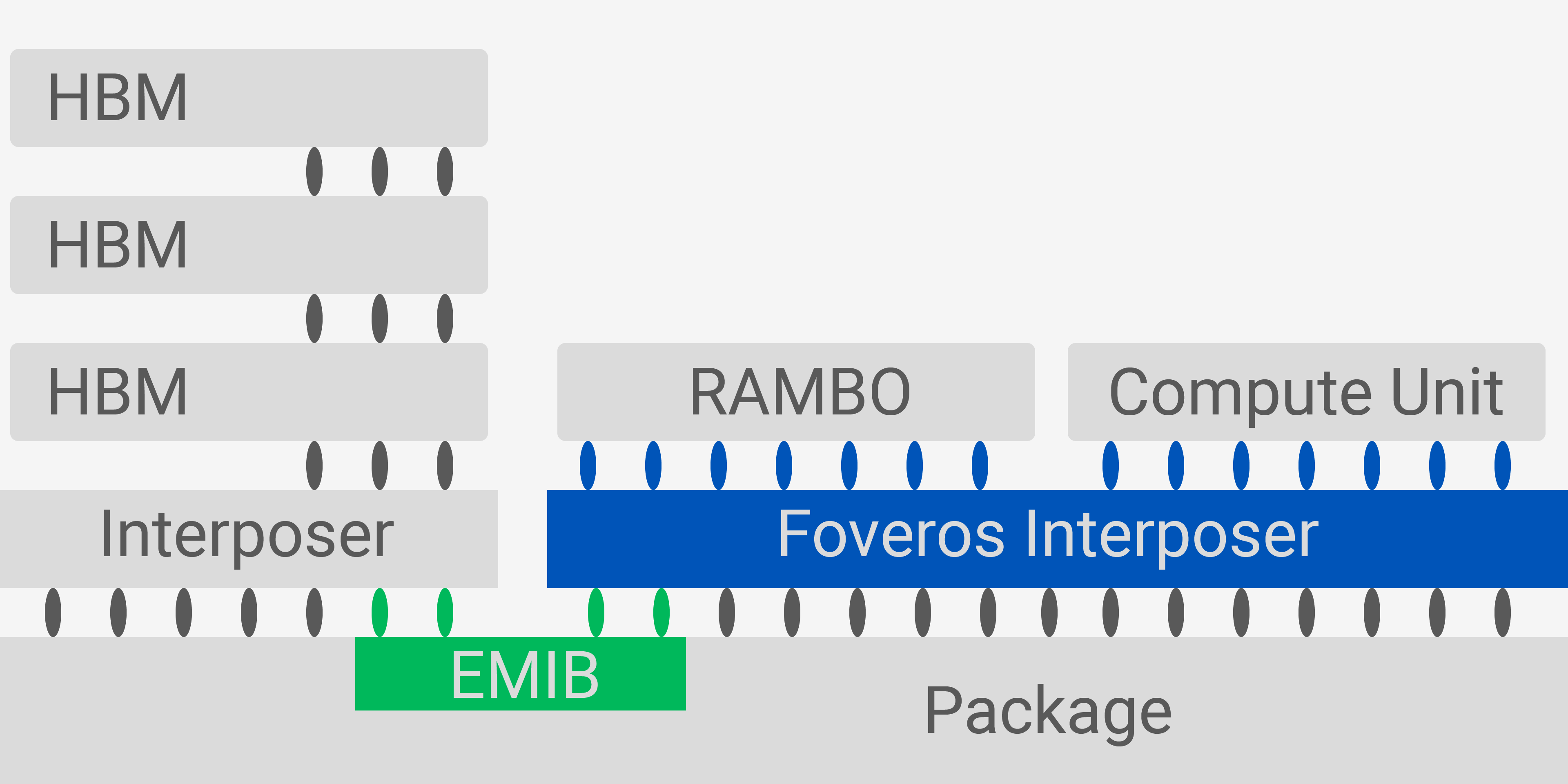
To do so, Ponte Vecchio leverages Intel's pivotal new interconnect technologies, Foveros and EMIB (embedded multi-die interconnect bridge). Foveros uses through-silicon vias to stack multiple chips on top of an active interposer die, giving them on-chip like speeds but off-chip connectivity. In comparison, EMIB is a 'dumb' connection between two chips that uses an inactive die but offers high bandwidth at a lower cost.
EMIB and Foveros
EMIB is used to connect the GPU's compute hardware directly to the HBM, netting Ponte Vecchio spectacular memory bandwidth. Foveros is used to connect the two CUs on a sub-slice to one chiplet of RAMBO cache, Intel's new super cache. Thanks to Foveros, RAMBO doesn't have any limitations imposed upon its capacity or footprint, and it can bypass the CUs when sending/receiving data from the HBM or other sub-slices.
Having a gigantic cache - and by gigantic I mean gigantic, Intel's diagrams show a RAMBO chiplet as being the same size as a CU - is obviously really expensive, but it unlocks some nifty options. In neural network processing, for example, RAMBO can store matrices an order of magnitude larger than other GPU caches. Other GPUs lose performance as matrices get larger and the level of precision increases, but Ponte Vecchio is able to sustain peak performance.
Ponte Vecchio
The RAMBO cache also powers the Xe Memory Fabric, a spiderweb of connections and technologies that pools resources from every GPU and CPU in a server node. Every GPU's RAMBO cache is combined into one bank available to everything, with the slowest connection being the CPUs' at 63 GB/s over PCIe 5.0.
At their recent yearly earnings investor meeting, Intel confirmed that Ponte Vecchio will begin shipping during the fourth quarter of 2021. It's unclear if that refers to a full release or an exclusive early launch for the Aurora supercomputer.
Software
Hardware is good and all, but completely useless without adequate software support. And the threshold is pretty high: if even 1% of games aren't properly supported, millions of gamers are alienated. The good news is Intel seems to be doing their best.
Intel is redesigning its lowest level of software, the instruction set architecture (ISA), for modern high-performance applications. "Gen12 is planned to include one of the most in-depth reworks of the Intel EU ISA since the original i965. The encoding of almost every instruction field, hardware opcode and register type needs to be updated."
At the driver level, Intel has a long way to go but is making progress. Their integrated GPU drivers aren't updated as frequently as their competitors', with the mean time between the last ten updates being 26 days for Intel versus 14 days for Nvidia and 12 days for AMD. But their stability and support did improve a lot during 2019, and 275 new titles were optimized for Intel's architecture.
Intel's consumer-facing software, on the other hand, is superb. Their recently released Graphics Command Center provides significantly more control than Nvidia's GeForce Experience, for example, and is easier to use. Like GeForce Experience, it can optimize games for particular hardware configurations, but it also explains what each setting does and how much of a performance impact it will have. Driver control is pleasantly straightforward.
The Command Center is unique in providing advanced display controls as well. It offers painless multi-display set up and refresh rate and rotation syncing, along with thorough options to adjust color styling. I personally use it to control my system, despite running Nvidia hardware.
As a bonus, Intel also supports variable refresh rate, so Xe products will support FreeSync and G-Sync monitors.
Release
While Intel is being a bit coy about what they'll announce at GDC in March, there's a good chance we're looking at a full reveal. If that's the case, then we can expect a release in the subsequent months. The most likely candidate is June.
Last October, Koduri tweeted a not-so-subtle hint in the form of an image of his new numberplate. It reads "Think Xe" and has a June 2020 date. He is refusing to comment on whether the date has any significance or not, which suggests it probably does.
One advantage of leaking a date in this manner is that it tells the community what to expect, without building so much excitement that fans will get angry if the GPUs arrive in July instead. So consider it a blurry target; Intel is probably aiming for a June release (in time for Computex), but it might take a little longer depending on how things are going.
Intel is hinting at some pretty cool stuff and we remain hopeful about having a third major player in the graphics arena. But until it's not time we can't be anything more than cautiously optimistic.
Shopping Shortcuts:
- AMD Radeon RX 5700 XT on Amazon, Google Express
- AMD Radeon RX 5700 on Amazon, Google Express
- GeForce RTX 2070 Super on Amazon, Google Express
- GeForce RTX 2060 Super on Amazon, Google Express
- GeForce RTX 2080 Ti on Amazon, Google Express
- AMD Ryzen 9 3900X on Amazon, Google Express
- AMD Ryzen 5 3600 on Amazon, Google Express
- AMD Ryzen 5 2600X on Amazon, Google Express


 -
-