What just happened? A team of researchers at MIT, in collaboration with Georgia Tech and the Air Force Research Laboratory, has developed a new method for integrating gallium nitride (GaN) transistors onto standard silicon chips. As the demand for faster and more efficient electronics continues to grow, this innovation represents a significant step toward bridging the gap between cutting-edge materials and mainstream technology.
Gallium nitride, a semiconductor renowned for its efficiency and high-speed capabilities, has long been recognized as a promising material for next-generation electronics, including power amplifiers that drive mobile phone signals and high-frequency components essential for data centers. However, the widespread use of GaN has been hindered by its high cost and the technical challenges associated with integrating it with conventional silicon-based electronics.
The new process, recently presented at the IEEE Radio Frequency Integrated Circuits Symposium, addresses these obstacles by introducing a scalable and cost-effective way to bond GaN transistors directly onto silicon chips. Traditionally, integrating GaN with silicon required either soldering, which limited the size and performance of the transistors, or bonding entire GaN wafers to silicon, a method that wasted large amounts of expensive material.
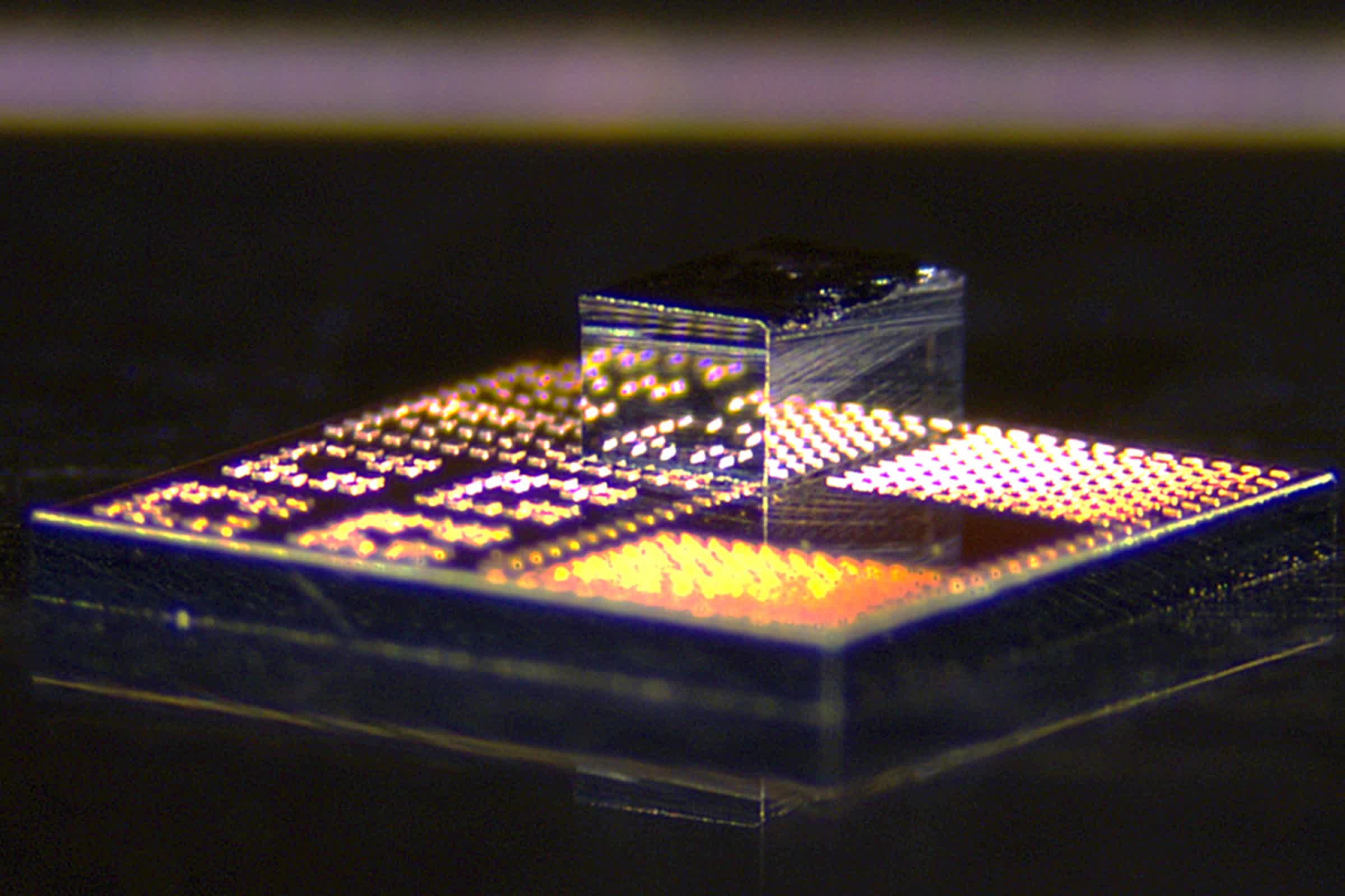
The MIT-led team's approach is different. They begin by fabricating thousands of tiny GaN transistors, each just a few hundred microns across, on a single wafer. These transistors are then precisely cut out and individually bonded onto a silicon chip only where they are needed, minimizing material use and cost.
The technical heart of the process lies in the use of copper-to-copper bonding. Each GaN transistor is equipped with microscopic copper pillars, which are aligned and pressed onto matching copper structures on the silicon chip. This bonding occurs at temperatures below 400 degrees Celsius, low enough to avoid damaging the delicate semiconductor materials.

Unlike older methods that relied on gold, which is expensive and requires higher temperatures, copper offers both affordability and superior electrical conductivity. The researchers developed a specialized tool to handle the tiny transistors, using vacuum suction and advanced microscopy to position each one with nanometer precision before bonding.
This method not only preserves the unique advantages of both GaN and silicon but also enables the integration of high-speed, high-efficiency transistors into existing chip designs without major changes to manufacturing processes.
In demonstration tests, the team created a power amplifier using their hybrid chips that outperformed traditional silicon-based devices in both bandwidth and signal strength. The compact design also helps reduce heat, a persistent challenge in high-performance electronics.
Beyond immediate applications in wireless communications and data centers, the researchers believe this technology could play a role in future quantum computing systems, where GaN's performance at extremely low temperatures offers distinct advantages over silicon.
Pradyot Yadav, an MIT graduate student and lead author of the study, explained that the goal was to combine the best features of GaN and silicon without compromising on cost or performance. By adding only the necessary GaN transistors to a silicon chip, the team achieved a balance between scalability and efficiency that could make advanced electronics more accessible and affordable.
The work was supported by the US Department of Defense and the Semiconductor Research Corporation, with fabrication carried out at MIT.Nano, the Air Force Research Laboratory, and Georgia Tech.
MIT researchers bond gallium nitride transistors to silicon for faster next-gen wireless devices
