In a nutshell: TSMC is venturing into uncharted territory with a novel approach to advanced chip packaging. The chipmaker reportedly plans to switch from conventional round wafers to rectangular substrates, allowing significantly more chips to be placed on each wafer.
The proposed rectangular substrate is currently undergoing trials. Measuring a substantial 510mm by 515mm, it reportedly boasts over three times the usable area of current round wafers. Additionally, the rectangular shape reduces wasted space around the edges. The study is still in the early stages, and its results may take a few years to reach the market.
Historically, substrates have been round due to their handling advantages and superior strength. However, the sudden interest in changing this trend is unsurprising given the AI boom. Like other chipmakers, TSMC is feeling the pressure from the skyrocketing demand for computing power and aims to keep pace.
It's fascinating to see how chip packaging, once considered the less glamorous side of chipmaking, has become crucial in advancing semiconductor technology.
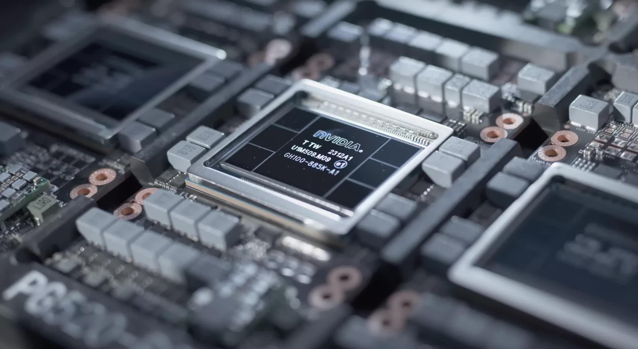
For instance, Nvidia's H200 and B200 AI computing chips rely on TSMC's state-of-the-art CoWoS (chip-on-wafer-on-substrate) technology. This advanced packaging method combines multiple processing units and high-bandwidth memories, resulting in faster data throughput and improved computing performance.
As chips grow larger to accommodate more transistors and memory, the current 12-inch wafer standard might not suffice in a couple of years. That's where TSMC's rectangular substrate experiment comes in.
However, this shift won't be a walk in the park. TSMC and its suppliers will need to invest significant time and resources into development. They'll also have to upgrade or replace a substantial amount of production tools and materials. One major hurdle is figuring out how to apply photoresists (light-sensitive materials used in chip manufacturing) on these new rectangular substrates, a chip executive told Nikkei Asia.
TSMC is not the only manufacturer experimenting with cutting-edge substrate technologies. Its biggest competitor, Samsung, is rumored to be investing heavily in research and development of glass substrates for chip manufacturing, with the goal of bringing products to market as early as 2026. Using glass offers several advantages compared to organic substrates, such as enhanced flatness, which improves the depth of focus for lithographic processes.
TSMC explores massive rectangular chip substrates to meet AI demand
")