A closer look to the Core i7 and Nehalem
The revamped architecture used on the new Core i7 is a whole new ball game, and as you are about to find out, much has changed.
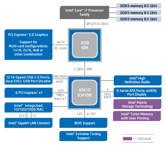
Possibly the largest architectural change involves the QuickPath Interface (QPI) which we mentioned earlier. The QPI has been developed to replace the aging FSB (Front Side Bus), offering a lightning fast interface between the CPU and the chipset. Of course, the chipset must support QPI technology and therefore the X48 has been replaced by the new X58 chipset.
Now, because components no longer run off a universal FSB which is then multiplied to get an intended frequency, Intel has introduced a single 133.33MHz base clock. Each component uses its own unique multiplier to reach a specified frequency. Take the Core i7 940 processor, which operates at 2.93GHz using a 22x multiplier (22 x 133 = 2926MHz).

However unlike conventional processors, which use a single multiplier, the Core i7 965 Extreme Edition for example offers a feature called "Turbo Mode". When enabled, this allows the user to designate an individual multiplier to each of the four processor cores. This means that when overclocking it is possible to push only the first core to the extreme as this is the most heavily used core. As a result you can reduce the heat output if only the core(s) in demand are running at their peak capacity, rather than all four.

The memory also works in a similar fashion, using a multiplier off the base 133.33MHz clock to achieve a certain frequency. For example, by default the Core i7 platform uses DDR3-1066 memory and to reach this frequency an 8x multiplier is required. This really simplifies overclocking and allows the user to either adjust the 133.33MHz base clock to overclock everything at once, or individually overclock components using their multiplier.
This simplified overclocking potential along with greater bandwidth between the processor and chipset are impressive enhancements, but there was something else the FSB was holding back. That is of course memory performance, and to solve this problem Intel has finally done what AMD did years ago, move the memory controller onto the CPU. The new on-die memory controller of the "Bloomfield" Core i7 processors supports triple-channel DDR3 memory.
Previously the 333MHz FSB of the high-end Core 2 processors limited them to a peak memory bandwidth of 10.6GB/s, while DDR2-1066 memory working in dual-channel mode had a peak bandwidth of 17GB/s. In order to move forward Intel had to remove the need for the FSB, and since AMD already had the answer, Intel just had to follow.
That's not to say Intel didn't think beyond, so they went all out developing a triple-channel DDR3 memory controller.

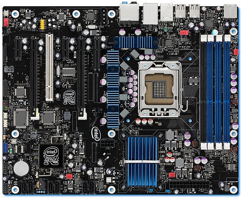
When paired with low-end DDR3-1066 memory this controller will have a peak bandwidth of 25.5GB/s, while DDR3-1333 will exceed 31GB/s! While the speed is impressive, also keep in mind this controller supports three channels and allows for two DIMMs per channel. This means that motherboards can have three or six DIMM slots instead of the usual two or four.
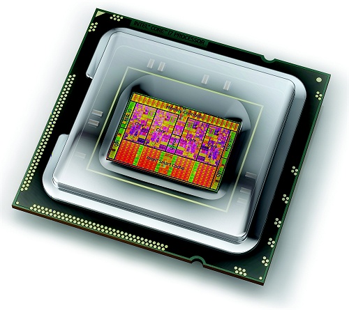
It should be pointed out as well that the Core i7 processors can only support DDR3 memory. The Core i7 is a single-die processor, meaning all four cores, the memory controller, and all cache are on a single die. The three processors that we are looking at today feature an on-die shared 8MB L3 cache, while each of the four cores have its own 256KB L2 cache. In total, each processor boasts an impressive 731M transistors and a thermal design process of 130W.
As the icing on the cake, hyper-threading technology makes a comeback on the Core i7, making these quad-core processors capable of handling a total of eight threads. This is the same feature that was present in the older Netburst Pentium 4 processors, but was dropped for the Core 2 line-up. Indeed, your OS will see eight cores.