Now that we know how processors work at a high level, it's time to dive deeper into their internal components and how they are designed. This article is the second part of our series on processor design. If you haven't read Part 1 yet, we recommend doing so first, as some of the concepts discussed here may not make sense otherwise.

Transistors: The Building Blocks of Processors
As you probably know, processors – and most other digital technology – are made up of transistors. The simplest way to think of a transistor is as a controllable switch with three pins. When the gate is on, electricity is allowed to flow through the transistor; when the gate is off, current cannot flow. It's similar to the light switch on your wall but much smaller, much faster, and electrically controlled.
Modern processors use two main types of transistors: pMOS and nMOS. An nMOS transistor allows current to flow when the gate is charged or set high, while a pMOS transistor allows current to flow when the gate is discharged or set low. By combining these two types of transistors in a complementary way, we can create CMOS logic gates. We won't go into the intricate details of how transistors work physically in this article, but we'll touch on it in Part 3 of the series.
A logic gate is a simple device that takes inputs, performs an operation, and outputs a result. For example, an AND gate turns its output on only if all its inputs are on. An inverter (or NOT gate) turns its output on only if the input is off. By combining these two, we can create a NAND ("not AND") gate, which turns its output on unless all inputs are on. Other logic gates include OR, NOR, XOR, and XNOR, each with different logical functions.
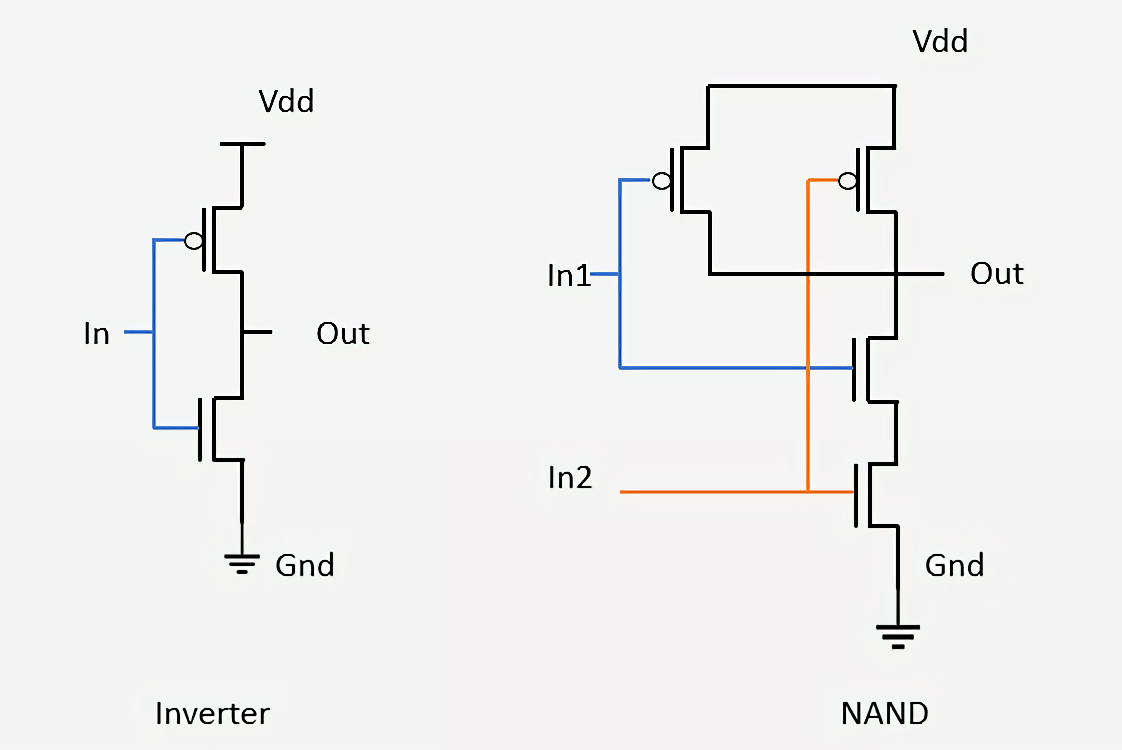
Above, we can see how two basic gates are constructed from transistors: an inverter and a NAND gate. In the inverter, a pMOS transistor is placed at the top, connected to the power line, while an nMOS transistor is at the bottom, connected to the ground. pMOS transistors are drawn with a small circle at the gate. Since pMOS devices conduct when the input is off and nMOS devices conduct when the input is on, the signal at Out will always be the opposite of the signal at In.
Looking at the NAND gate, we see that it requires four transistors and that the output remains on as long as at least one of the inputs is off. This same principle is used to design more advanced logic gates and other circuitry within processors.
From Logic Gates to Functional Units
With building blocks as simple as logic gates, it can be difficult to see how they are transformed into a functioning computer. This design process involves combining multiple gates to create a small device that performs a specific function. These small devices are then connected to form more complex functional units, ultimately leading to a fully operational processor. The process of integrating these individual components is the same method used to build modern chips – the only difference is that today's chips contain billions of transistors.
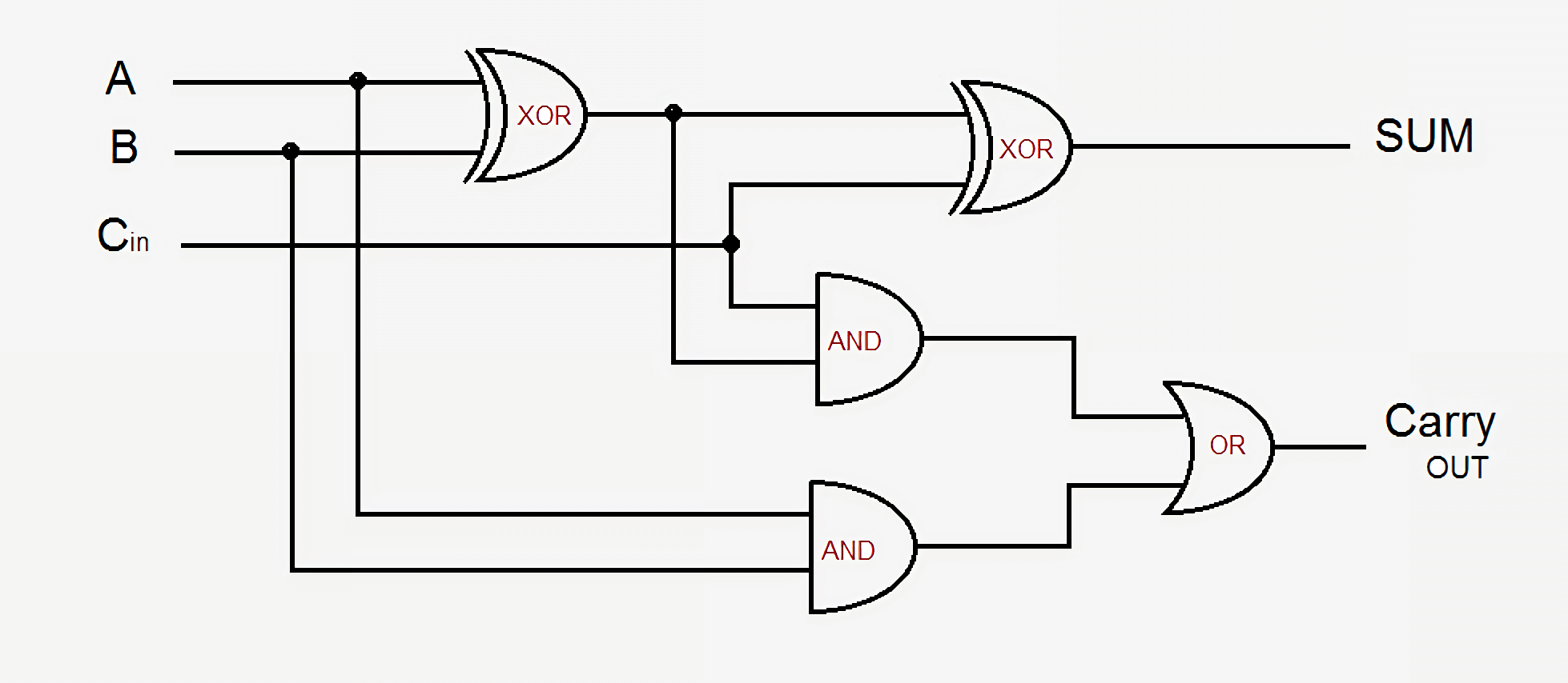
As a quick example, let's look at a 1-bit full adder. This circuit takes three inputs (A, B, and Carry-In) and produces two outputs (Sum and Carry-Out). The basic design consists of five logic gates, and multiple adders can be linked together to create an adder of any desired size. Modern designs improve on this by optimizing logic and carry signals, but the fundamental principles remain the same.
The Sum output is on if either A or B is on – but not both – or if there is a carry-in signal while A and B are both on or both off. The Carry-Out signal is slightly more complex: it is active when both A and B are on, or if there is a carry-in and one of A or B is on. To connect multiple 1-bit adders and form a wider adder, we simply connect the Carry-Out of the previous bit to the Carry-In of the current bit. The more complex the circuits get, the messier the logic gets, but this is the simplest way to add two numbers. While modern processors use more advanced adders, the fundamental concept remains the same.
Modern processors use more complex adders, but those designs are too complicated for an overview like this. In addition to adders, processors also contain units for division, multiplication, and floating-point versions of all of these operations.
Combining a series of gates like this to perform some function on inputs is known as Combinational Logic. This type of logic isn't the only thing found in computers though. It wouldn't be very useful if we couldn't store data or keep track of the state of anything. To do this, we need sequential logic which has the ability to store data.
Storing Data: SRAM and DRAM
Sequential logic is built by carefully connecting inverters and other logic gates such that their outputs feed back to the input of the gates. These feedback loops are used to store one bit of data and are known as Static RAM or SRAM. It is called static RAM, as opposed to dynamic in DRAM, because the data being stored is always directly connected to positive voltage or ground.
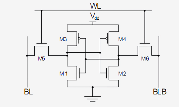
A standard way to implement a single bit of SRAM is with 6 transistors shown below. The top signal, marked WL for Word Line, is the address and when it is enabled, the data stored in this 1-bit cell is sent to the Bit Line, marked BL. The BLB output is known as Bit Line Bar, is just the inverted value of Bit Line. You should be able to recognize the two types of transistors and that M3 and M1 form an inverter along with M4 and M2.
SRAM is used to build the super-fast caches and registers inside processors. It is very stable but requires six to eight transistors to store each bit of data. This makes it extremely expensive to produce in terms of cost, complexity, and chip area compared to DRAM.
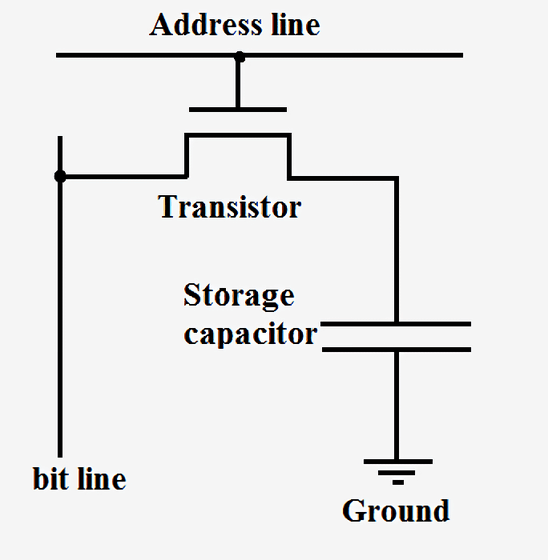
Dynamic RAM, on the other hand, stores data in a tiny capacitor rather than using logic gates. It is called dynamic because the voltage of the capacitor can change dynamically since it is not connected to power or ground. A single transistor is used to access the data stored in the capacitor.
Because DRAM only requires a single transistor per bit and has a highly scalable design, it can be packed densely and produced at a lower cost. However, one drawback to DRAM is that the charge in the capacitor is so small that it needs to be refreshed constantly. This is why when you turn off your computer, the capacitors drain, and the data in your RAM is lost.
Companies like Intel, AMD, and Nvidia certainly don't release schematics detailing how their processors work, so it's impossible to show full diagrams of a modern processor. However, this simple adder should give you a good idea of how even the most complex parts of a processor can be broken down into logic gates, storage elements, and transistors.
Clock Signals and Frequency
Now that we know how some processor components are constructed, we need to figure out how to connect everything and synchronize it. All key components in a processor are connected to a clock signal, which alternates between high and low at a predefined interval known as the frequency. The logic inside a processor typically switches values and performs calculations when the clock goes from low to high. By synchronizing everything, we ensure that data arrives at the correct time, preventing glitches in the processor.
You may have heard that increasing a processor's clock speed – known as overclocking – can improve performance. This performance gain comes from switching the transistors and logic inside a processor faster than it was originally designed for. Since there are more cycles per second, more work can be completed, resulting in higher performance. However, this only works up to a certain point.
Modern processors typically run between 3.0 GHz and 5.0 GHz, and this range has remained largely unchanged over the past decade. Just like a metal chain is only as strong as its weakest link, a processor can only run as fast as its slowest part. By the end of each clock cycle, every single component in a processor must have finished its operation. If any parts are still processing, the clock is too fast, and the processor won't work. Designers refer to this slowest part as the Critical Path, which determines the maximum frequency a processor can run at. Above a certain frequency, the transistors simply cannot switch fast enough, leading to glitches or incorrect outputs.
Increasing the supply voltage to a processor can speed up transistor switching, but only to a certain extent. If too much voltage is applied, the processor risks overheating or burning out. Raising the frequency or voltage will always result in more heat generation and higher power consumption. This is because processor power is directly proportional to frequency and proportional to the square of the voltage. To estimate the power consumption of a processor, each transistor can be thought of as a small capacitor that must be charged or discharged whenever it changes state.
Power Management and Efficiency
Power delivery is such a critical aspect of processor design that, in some cases, half of a chip's physical pins are dedicated solely to power or ground. Some chips may draw more than 150 amps at full load, and all that current must be carefully managed. To put this into perspective, a CPU generates more heat per unit area than a nuclear reactor.
The clock signal in modern processors accounts for roughly 30-40% of total power consumption since it is highly complex and must drive multiple components simultaneously. To conserve energy, most low-power designs turn off portions of the chip when they are not in use. This can be done by shutting off the clock, a technique known as Clock Gating, or by cutting off power entirely, known as Power Gating.
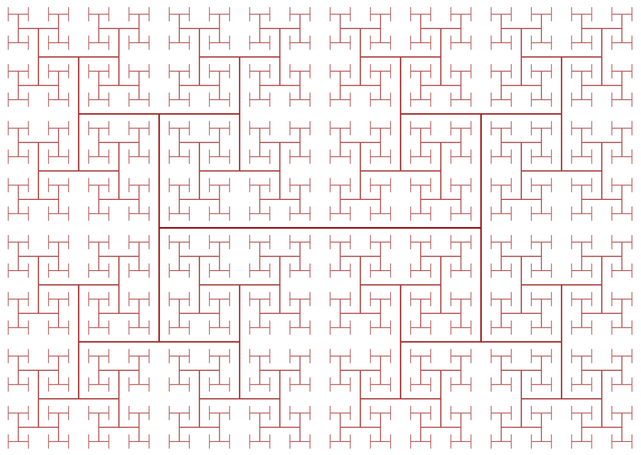
Clocks present another challenge in processor design because, as their frequencies increase, the laws of physics start to interfere. Even though the speed of light is incredibly fast, it is not fast enough for high-performance processors. If the clock signal were sent from one end of the chip to the other, by the time it reached the farthest point, it would be out of sync. To ensure all portions of the chip remain in time, the clock is distributed using a structure known as an H-Tree (above). This ensures that all endpoints are the exact same distance from the center, maintaining synchronization across the chip.
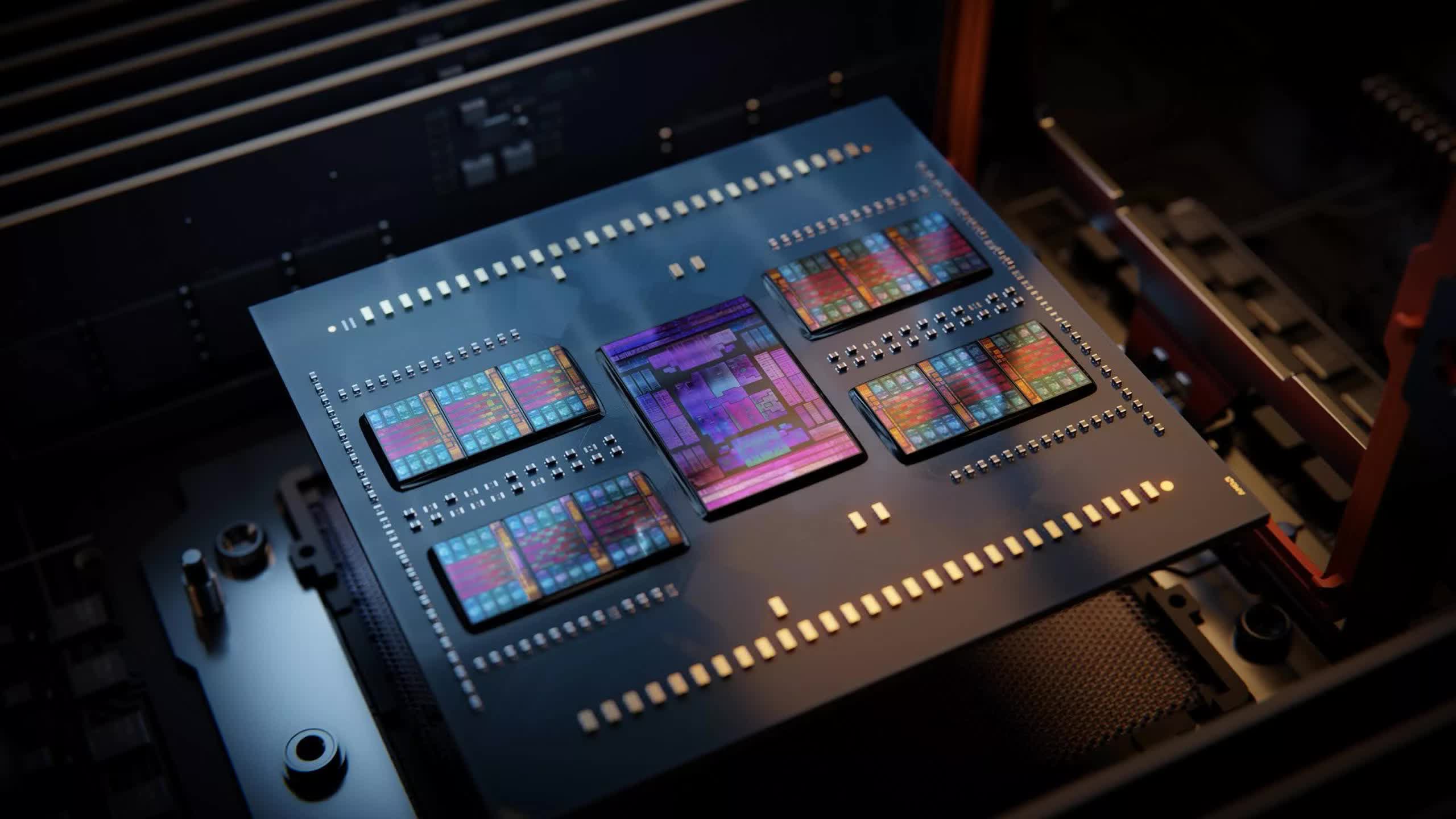
Speaking of efficiency, modern processors are becoming increasingly power-hungry. To address this, many designers are adopting chiplets in addition to optimizing performance on a single chip (see our full explainer on chiplets here). Chiplets are segmented processors, meaning that instead of consolidating every component into a single monolithic chip, different sections are manufactured as separate smaller chips. For example, a CPU may have separate efficient cores and power cores that can be turned on or off depending on the workload. This modular approach allows the components that benefit most from the latest fabrication methods to be shrunk, improving manufacturing efficiency and enabling more components to fit within the same processor.
How Processors Are Designed
It may seem extremely tedious and complex to design every single transistor, clock signal, and power connection in a chip, and that would certainly be true. Even though companies like Intel, Qualcomm, and AMD have thousands of engineers, it would not be possible for them to manually design every aspect of a chip. To put together chips on such a scale, they use a variety of advanced tools to generate the designs and schematics for them.
These tools will typically take a high-level description of what the component should do and determine an optimal hardware configuration to meet those requirements. There has been a growing shift towards High-Level Synthesis (HLS), which allows developers to specify the functionality they want in code, and then have computers figure out how to optimally implement it in hardware. This abstraction not only accelerates development but also enables faster iterations and optimizations at scale.
More recently, AI-driven design techniques have started to revolutionize chip development. Companies like Google, Nvidia, and Synopsys have integrated machine learning models into chip layout and floorplanning, dramatically reducing the time required to place billions of transistors efficiently. AI is now playing a role in optimizing power efficiency, timing analysis, and even automated bug detection – helping engineers identify design flaws before fabrication.
Verification in Processor Design
Just like you can define computer programs through code, designers can also define hardware through code. Languages such as Verilog and VHDL allow hardware designers to express the functionality of whatever circuit they are making. Simulation and verification are performed on these designs, and if everything passes, they can be synthesized down into the specific transistors that will make up the circuit. While verification may not seem as flashy as designing a new cache or core, it is considerably more important.
Verification of a new design often takes much more time and money than building the actual chip itself. Companies spend so much time and money on verification because once a chip goes into production, there's no way to fix it. With software you can just issue a patch, but hardware doesn't work that way for the most part.
For example, Intel had a bug in the floating point division unit of some Pentium chips back in the late 1990s, which ended up costing them the equivalent of $2 billion today. Conversely, we've seen many cases of security bugs in chips in the last decade, some of which has been remedied by manufacturer-issued microcode and firmware updates. However, these fixes have come at the cost of diminished performance or brand reputation.
It can be difficult to wrap your mind around how one chip can have several billion transistors and what they all do. When you break down the chip into its individual internal components, it gets a bit easier. Transistors make logic gates, logic gates are combined into functional units that perform a specific task, and these functional units are connected together to form the computer architecture we talked about in Part 1.
Much of the design work is automated, and with AI-driven tools now accelerating key aspects of chip development, the complexity of modern processors continues to grow. Still, this should give you a new appreciation for just how intricate and sophisticated that new CPU you bought really is.
This second installment covered the CPU design process. We talked about transistors, logic gates, power and clock delivery, design synthesis, and verification. In Part 3 we'll see what is required to physically build a chip. Each company likes to brag about how advanced their fabrication process is (think nanometers), but what do those numbers actually mean? Read on.
Masthead credit: Circuit board futuristic by Kirill Savenko

