Breakthrough CRAM technology ditches von Neumann model, makes AI 1,000x more energy efficient

zohaibahd

Posts: 934   +19
Staff
Futurology: The global demand for AI computing has data centers consuming electricity like frat houses chug beer. But researchers from the University of Minnesota might have a wildly innovative solution to curb AI's growing thirst for power with a radical new device that promises vastly superior energy efficiency.

The researchers have designed a new "computational random-access memory" (CRAM) prototype chip that could reduce energy needs for AI applications by a mind-boggling 1,000 times or more compared to current methods. In one simulation, the CRAM tech showed an incredible 2,500x energy savings.

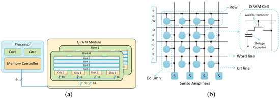
Traditional computing relies on the decades-old von Neumann architecture of separate processor and memory units, which requires constantly moving data back and forth in an energy-intensive process. The Minnesota team's CRAM completely upends that model by performing computations directly within the memory itself using spintronic devices called magnetic tunnel junctions (MTJs).

Rather than relying on electrical charges to store data, spintronic devices leverage the spin of electrons, offering a more efficient substitute for traditional transistor-based chips.

"As an extremely energy-efficient digital-based in-memory computing substrate, CRAM is very flexible in that computation can be performed in any location in the memory array. Accordingly, we can reconfigure CRAM to best match the performance needs of a diverse set of AI algorithms," said Ulya Karpuzcu, a co-author on the paper published in Nature. She added that it is more energy-efficient than traditional building blocks for today's AI systems.

By eliminating those power-hungry data transfers between logic and memory, CRAM technologies like this prototype could be critical for making AI vastly more energy efficient at a time when its energy needs are exploding.

The International Energy Agency forecasted in March that global electricity consumption for AI training and applications could more than double from 460 terawatt-hours in 2022 to over 1,000 terawatt-hours by 2026 – nearly as much as all of Japan uses.

The researchers stated in a press release that the foundations of this breakthrough were over 20 years in the making, going back to pioneering work by engineering professor Jian-Ping Wang on using MTJ nanodevices for computing.

Wang admitted their initial proposals to ditch the von Neumann model were "considered crazy" two decades ago. But the Minnesota team persisted, building on Wang's patented MTJ research that enabled magnetic RAM (MRAM) now used in smartwatches and other embedded systems.

Of course, as with any breakthrough of this sort, the researchers still need to tackle challenges around scalability, manufacturing, and integration with existing silicon. They're already planning demo collaborations with semiconductor industry leaders to help make CRAM a commercial reality.

Permalink to story:

 
Interesting as a research project, probably not as a commercial product any time soon. Being generous, there is 67,000 square millimeters available on a 300mm wafer but typically less. A 450um by 400um junction is 0.18mm^2, so a max of ~372k of these MJTs on a wafer assuming absolutely nothing else is there.

The math doesn't math here. The researchers need to release more data or I am unconvinced this even has the potential to ever become economically feasible. Useful in getting further funding for them sure, but this is far from reality still. A 1000x speedup means nothing if you have a 100,000x reduction in bit equivalence.
 
It's hardly a new idea. There's been many grid based processing arrays that have their own local RAM per processor. Hell, the Playstation 3 was built around that idea but it wasn't even close to the first.

The only possible new idea here is the possibility of adding MRAM fabrication to general logic fabrication production. Normally local RAM is built from SRAM. MRAM certainly has the density advantage over SRAM. They don't really say a lot about doing such though. It seems more just about ideas only.
 
What everything's gotta do with AI today? This smells like marketing research more than actual scientific paper. AI is a subset of computation world, not supersedes it.
My thought as well. The idea of C-RAM, as stylized on Wikipedia, would be far more general purpose than AI. That said, I skimmed the article, and while it mentions "machine intelligence" in a few places, very little of the paper discusses AI. So, this isn't for the AI marketing fad per se. Indeed, they studied gates which would serve as the "building blocks for many conventional and machine intelligence applications". The main reason the researchers mentioned machine learning seems to be this bit: "For now, while the error rate of CRAM is still higher compared to that of CMOS logic circuits, CRAM is naturally more suitable for applications that require less precision but can still benefit from the true-in-memory computing features and advantages of CRAM, instead of those that require high precision and determinism." In other words, AI, which notably use quantization these days to trade off precision for speed.
 
Oh, maybe they're implying a possible path to building neural nets in a fine grained fashion. Ie: A true analogue of brains where neurons are also the physical processor elements.

Problem there is fine grain functions have a routing issue. A real brain can grow new routes. Silicon hardware doesn't have that option. Best that exists there is FPGA structures where there is a set amount of excess routing resources. It's not very space efficient nor great for speed since every optional route is another mux and another point of heating. And the extended distances are an additional source of heating from capacitive loading. Not unlike the complaint the article is highlighting when using external RAM.

Throwing MRAM at this doesn't resolve the fine grain design issue.
 
What everything's gotta do with AI today? This smells like marketing research more than actual scientific paper. AI is a subset of computation world, not supersedes it.
This advance isn't limited to AI at all; it applies to all computation. The near century-old Von Neumann model is inherently inefficient. This has the capability to supplant that.

there is 67,000 square millimeters available on a 300mm wafer but typically less. A 450um by 400um junction is 0.18mm^2, so a max of ~372k of these MJTs on a wafer
The researchers chose a large (I.e. cheap and simple) node to demonstrate proof of concept. There's no reason these MJTs can't be fabricated far smaller -- Everspin, for instance, has for many years been making (very similar) STT-MRAM on the 28 nm node.

A 1000x speedup means nothing if you have a 100,000x reduction in bit equivalence.
It most certainly does when it comes with a 2500X boost in energy efficiency. And not just for AI, but for IOT devices as well, where the computation is very lightweight, but increasing battery life from a from a few hours to a year or more is game-changing.
 
This advance isn't limited to AI at all; it applies to all computation. The near century-old Von Neumann model is inherently inefficient. This has the capability to supplant that.
There is no diagram of how such a replacement functions though. It's just a claim without substance.

It most certainly does when it comes with a 2500X boost in energy efficiency. And not just for AI, but for IOT devices as well, where the computation is very lightweight, but increasing battery life from a from a few hours to a year or more is game-changing.
I haven't seen anything in the engineering that suggests any advance on power efficiency. It's just a claim in the ether.
 
There is no diagram of how such a replacement functions though. It's just a claim without substance.
On the contrary, not only does the Nature article clearly explain it, but this CRAM is just a type of memristor ... and we've been talking for 40 years about how a viable memristor component would revolutionize computing. Calling this a 'claim without substance' is far off base, when they actually built and tested an experimental full adder.

It's easy to understand how this new paradigm saves so much energy. To add two bytes stored on the drive of a traditional Von Neumann device, the values must first be loaded into RAM, then into the CPU's L3 cache -> L2 cache -> L1 cache -> then into registers, where they can finally be operated upon -- then walk that process backwards to store the result.
With a CIM (compute-in-memory) approach like CRAM, you can operate on those two values directly.
 
MRAM is certainly not memristor. Memristors are known for, like Flash, limited endurance therefore, like Flash, is only useful as a ROM tech. MRAM will have been chosen because it is the only NV option for unlimited endurance.

Right, found the diagram I think - https://www.nature.com/articles/s44335-024-00003-3/figures/2
Pity that one wasn't prominently displayed in this news item.

Hmm, it all looks like more address buses. Lots of added excess routes like FPGAs. Maybe that is an improvement, dunno. FPGAs stopped doing fine grained logic like that back in the 1990s. The routing became too bulky I suspect.
 
MRAM is certainly not memristor. Memristors are known for, like Flash, limited endurance therefore, like Flash, is only useful as a ROM tech.
Oops! This isn't MRAM, it's CRAM. It's MJT based, yes, but it also performs computation. It's right there in the title of the article itself:

"Experimental demonstration of magnetic tunnel junction-based computational random-access memory...."

And, according to Dr. Chua of Berkeley (among others):


And, while you might find others who claim CRAM isn't technically a memristor, it indisputably fills the same computational function as a memristor -- which is what's relevant in this context. It is memory that performs in-situ computation.
 
Last edited:
It is MRAM for the memory itself. The only alternates are SRAM or DRAM. The reason they've changed the name is because of the extra addressing lines and attached select transistors to get the logic function on a per cell basis. That's all they're promoting at all here - the added logic function - that is their "breakthrough."

Memristor is just another NV memory type like Flash or FRAM, all of which have limited endurance. And therefore don't have the ability to perform as RAM.
 
It is MRAM for the memory itself. The only alternates are SRAM or DRAM.
Or FRAM. Or PCM. Or ReRAM. Or many others. I've already given you a quote from Dr. Chua -- the man who coined the term "memristor" himself -- that this is indeed a memristor. It is the long-predicted missing fourth basic electronic circuit element.

..."Chua in his 1971 paper identified a theoretical symmetry between the non-linear resistor (voltage vs. current), non-linear capacitor (voltage vs. charge), and non-linear inductor (magnetic flux linkage vs. current). From this symmetry he inferred the characteristics of a fourth fundamental non-linear circuit element, linking magnetic flux and charge, which he called the memristor...."


Memristor is just another NV memory type...
While MJT junctions have previously been used only for NV memory, the fact that they could also perform direct computational functions was long known. Now it's been experimentally demonstrated. The first paper I read on memristor-based non Von-Neumann computation was in the early 1980s.
 
All memory types can be used for cell based logic. But only unlimited endurance of SRAM/DRAM/MRAM is worth pursuing. All other memories are technically ROMs.
 
All MRAM have a transistor with the MTJ. It isn't just the MTJ by itself.

A quote from the Nature article itself - "The MTJ, one of the transistors, word line (WL), bit select line (BSL), and memory bit line (MBL) resemble the 1T1M cell architecture of STT-MRAM, which allows the CRAM to perform memory operations."
 
All memory types can be used for cell based logic.
No. You can't perform direct logic operations on cells in traditional memory.

But only unlimited endurance of SRAM/DRAM/MRAM is worth pursuing. All other memories are technically ROMs.
The distinction between RAM and ROM isn't lifespan based. Furthermore, neither SRAM nor DRAM has "unlimited" endurance (on the order of 10E12 cycles), whereas MRAM has now surpassed the trillion-cycle endurance mark, more than enough for many applications.

All MRAM have a transistor with the MTJ. It isn't just the MTJ by itself.
No one said otherwise. It's MJT-based, not a naked magnetic junction.

A quote from the Nature article itself - "The MTJ, one of the transistors, word line (WL), bit select line (BSL), and memory bit line (MBL) resemble the 1T1M cell architecture of STT-MRAM, which allows the CRAM to perform memory operations."
If you missed that memristors perform memory functions, the "mem-" prefix might have alerted you.
 
You do realise SRAM is what CPUs and GPUs are built out of, right?
Not quite. Registers and cache are SRAM based, but "CPUs and GPUs" contain much more circuitry than that. Nor does that imply they have "unlimited" endurance -- even a simple CMOS flip-flop eventually experiences a hard error. And DRAM has a hard error rate at least an order of magnitude higher than SRAM.

In any case, you're now wading through the weeds. The original points stand. This CRAM is indeed a type of memristor, and their stated performance and efficiency gains are not smoke and mirrors: they've been experimentally verified. All that remains to be seen is, when manufactured on a modern process node, do they have a high enough density and low enough error rate to be feasible.
 
No. You can't perform direct logic operations on cells in traditional memory.
You can if it was added to each cell. Which is exactly what has been done here.
SRAM + logic is basically what the fine grained XC6000 FPGA was.
 
Not quite. Registers and cache are SRAM based, but "CPUs and GPUs" contain much more circuitry than that. Nor does that imply they have "unlimited" endurance -- even a simple CMOS flip-flop eventually experiences a hard error.
Endurance of SRAM can exceed 10E12 in a few hours. No, a flip-flop doesn't eventually wear out at all. If it fails then that wasn't from wear.
 
... and their stated performance and efficiency gains are not smoke and mirrors: they've been experimentally verified.
I said the only "breakthrough" is adding simple logic function to the basic MRAM cell.
As for performance, dunno, maybe it can do better than the past attempts at fine grained logic/memory mix.
 
You can if it was added to each cell. Which is exactly what has been done here.
SRAM + logic is basically what the fine grained XC6000 FPGA was.
Again -- not quite, no. The XC6000 line didn't add calculation logic to each cell, it (like all other fine-grained FPGAs) attached a number of logic blocks to a larger number of cells -- the 6264, for example, had 512 blocks for 16K cells, a 32:1 ratio.


Taken to the extreme, you would indeed get one logic block per memory cell ... but doing that with CMOS flip-flops would require ~100X the circuitry per cell as this memristor approach. The CRAM in the paper implements a memory AND computational logic cell using just two transistors and 1 magnetic junction.

Endurance of SRAM can exceed 10E12 in a few hours. No, a flip-flop doesn't eventually wear out at all.
Yes, flip-flops can and do eventually degrade, as do all CMOS circuitry. My 10E12 cycle figure (which is based on write switches, not reads) was for DRAM, which degrades at least an order of magnitude faster:

"Abstract: The cells in dynamic random access memory (DRAM) degrade over time as a result of aging....Commonly found wear-out failure mechanisms [are] bias temperature instability (BTI), hot carrier injection (HCI), time-dependent dielectric breakdown (TDDB)...An integrated circuit’s performance slowly but gradually degrades over time due to such wear-out phenomena. The degradation rate might depend on the switching activity, the gate voltage, the content of the DRAM cell, and several other factors...."

 
The XC6000 line didn't add calculation logic to each cell, it (like all other fine-grained FPGAs) attached a number of logic blocks to a larger number of cells -- the 6264, for example, had 512 blocks for 16K cells, a 32:1 ratio.
The "function unit" is the basic cell. Everything else is just routing.
 
Back