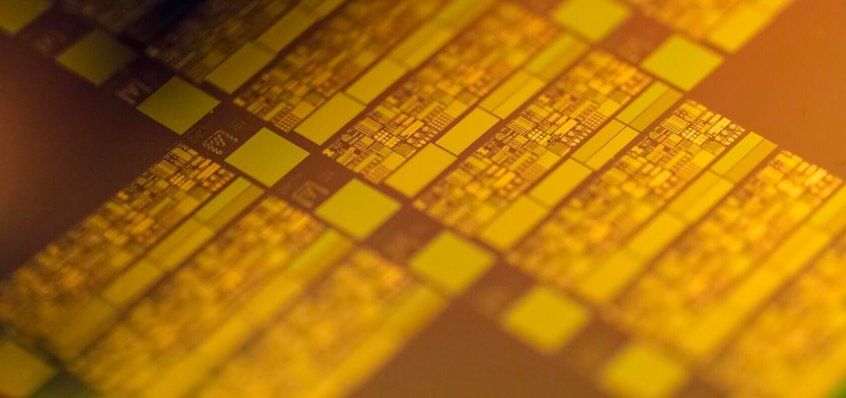
How CPUs are Designed and Built, Part 3: Building the Chip

I would like to thank you for doing this "How CPUs are designed" series.

I am versed in all of this, but I have been able to link these to others for insightful reading. Which sparked many discussions over the last month or so.
 
I knew a guy that owned a company that made machines that would test the wafers. If he was still alive today I could have probably found out actual yields.

Now lets talk about how to program processors! XD
 
Interesting how they use one big wafer.
My 720 X3 ran with the 4th core unlocked at 3.5GHz for years, my Heka turned Denab.
Once in awhile it would crash but it was seldom.
 
The Build, this was the coolest part to read so far. I hate to ask the dumb question but being just a consumer I have to ask. You said here defects are the limiting factor in chip size. Do you think the chip makers are secretly working on using binning, to side step the chip size issue? Sort of take the cream, designed to be put together by another process to make one custom built, snap together super big cpu block lol?

That would be so cool if they were doing that kind of stuff!
 
Last edited by a moderator:
The Build, this was the coolest part to read so far. I hate to ask the dumb question but being just a consumer I have to ask. You said here defects are the limiting factor in chip size. Do you think the chip makers are secretly working on using binning, to side step the chip size issue? Sort of take the cream, designed to be put together by another process to make one custom built, snap together super big cpu block lol?

That would be so cool if they were doing that kind of stuff!


Nope, did you notice how small those dies were, on those wafers..?

They were much smaller than the mega-chips from years ago, or Nvidia's Volta chip w/21 billion transistors...!! = about as big as you can go, without having difficulties with having all those billions of transistors etched perfectly within a CPU/GPU die. Effecting yield of how many (per wafer) come out perfect.

In contrast to having much smaller chips with 12 billion transistors/etc.. and having much better yield of good chips per wafer... and not only that, but able to fit more than double the chips on a wafer, vs 21 billion sized chip.


Understand, in the real world of analytics/science, etc, you don't need one GPU die with 100 billion transistors, when you only need to link 5 GPUs together that have 21 billion... and have the same compute.
 
"When looking at these numbers, it's important to note that some companies may base their process size on different dimensions than the standard width. "

At this point the process name is just a marketing term and doesn't actually reflect anything other than the relative density of the process.
 
Brilliant read. As a coder I am always interested to see how the CPU works. You have got me thinking now about how my C or ASM commands look inside the CPU, Going to see if I can find some visualisations on this.
 
Back