Nvidia's first Ampere GPU is a silicon monster for AI and servers

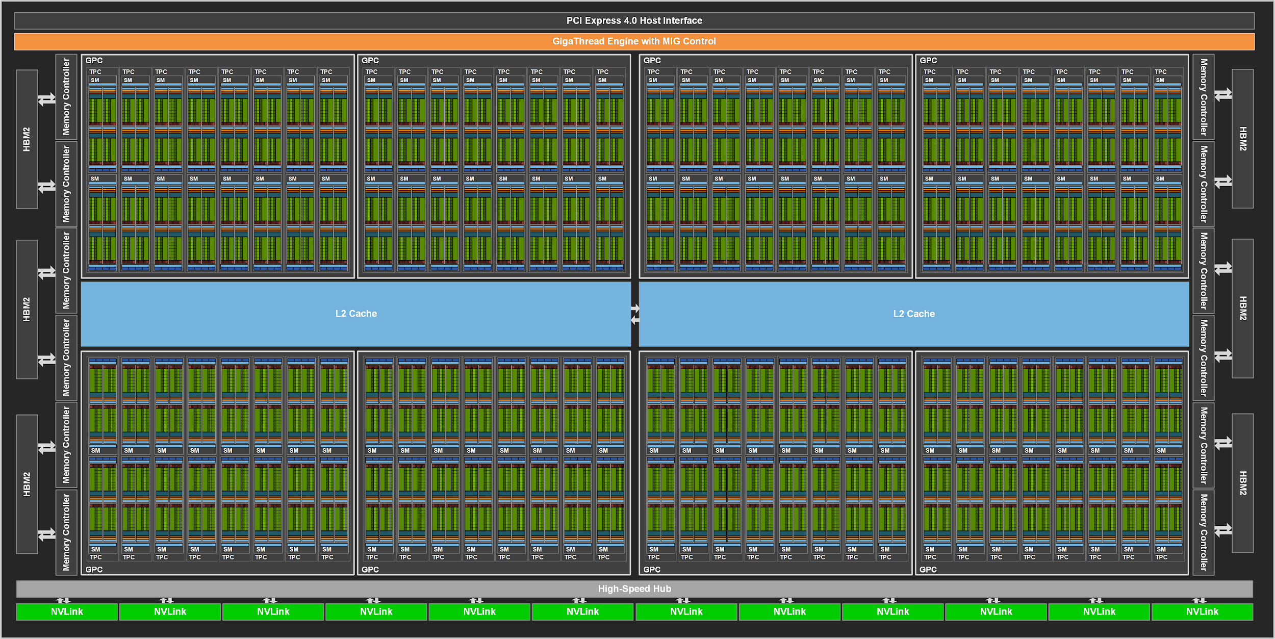
It's even more impressive when you realise that the stated die areas includes the HBM/HBM2.

The bulk of the changes lies within the tensor cores, of course, but the rest of the chip is essentially 'big-Volta', I.e. more SMs, more cache (a lot more L2, over 6 times more), more memory controllers, more NV Links:

Biggest question for me is how is this all going to get scaled down to keep the power consumption sensible: the A100's TDP is 400W, which is 150W more that the Tesla V100 SXM2 32GB. Obviously dropping the HBM2 will help quite a bit, as will hoofing off a few SMs, but it's still going to be high. 300W maybe?

Given that tensor cores only do matrix FMA, this is unlikely. The RT cores are specialised ASICs, two in fact: one for handling ray-triangle intersection calculations and the other for accelerating BVH algorithms. The tensor cores are used for denoising the images - but given that Ampere's are far more capable than Turing's, we're more likely to just see fewer TCs per SM, to allow for more RTCs. Or now that DLSS is TC-based, we could see this being pushed far more to offset the RT performance hit.

Now there is some confusion, I don't think the 826mm2 die size include the HBM2 at all, 826mm2 is the GPU die size alone.
Looking at the Vega Frontier Tear-down, the total size of the interposer + GPU is 30x30mm (900mm2), while the reported die size is ~495mm2 (20x26mm as measured by GamerxNexus). Each HBM stack is around 120mm2.

Nvidia can just use a lower voltage to improve efficiency on Ampere, as they had been doing with Turing.

Oh looking at A100 TC can do FP32 so I took that into the RTX-OPS calculations, but let say RT calculations are done on shader cores as with Pascal and Volta, the A100 already has higher RTX-OPS than 2080 Ti without any RTC (19.5 x 0.8) + (19.5 x 0.28) + (312 x 0.2) = 83.46 Tera RTX - OPS
 
Last edited:
Looking at the Vega Frontier Tear-down, the total size of the interposer + GPU is 30x30mm (900mm2), while the reported die size is ~495mm2 (20x26mm as measured by GamerxNexus). Each HBM stack is around 120mm2.
Good to know - thanks (y) (Y)

Oh looking at A100 TC can do FP32 so I took that into the RTX-OPS calculations, but let say RT calculations are done on shader cores as with Pascal and Volta, the A100 already has higher RTX-OPS than 2080 Ti without any RTC (19.5 x 0.8) + (19.5 x 0.28) + (312 x 0.2) = 83.46 Tera RTX - OPS
The FP32 format for the new tensor cores only kicks in automatically if the calculation is a matrix multiply-accumulate (what Nvidia calls a tensor calculation); FP32 vector operations are done via the usual CUDA cores. It will be interesting to see how much work the drivers (or more rather, the SM schedulers) will be able to push onto the tensor cores.

Nvidia has said this about the A100:
Because the A100 Tensor Core GPU is designed to be installed in high-performance servers and data center racks to power AI and HPC compute workloads, it does not include display connectors, NVIDIA RT Cores for ray tracing acceleration, or an NVENC encoder.
Your point about the TC's capabilities is a good one, but it's unlikely that they will abandon all of the work done creating the custom ASICs and software routines in the drivers after just one generation of use.
 
More than doubled the transistors of the old 12nm Tesla V100 on a die basically the same size.

21Bn v 54Bn.

That's all I needed to know for now to see the potential of consumer Ampere. Double the transistor density of existing Turing parts. Swish.
 
Note that my score is slightly above a desktop ave with the same CPU\GPU combo. And you can usually add 5 to 10% once optimus is bypassed with an external monitor.

I also ran the 3dMark stress test (40 passes) and the 2080 temps peaked at 64C.
I mean, I have a desktop 8700k and 1080Ti and my score was 23609. Yours really isn't that impressive. In fact, you can easily see on the 3Dmark website that most people with a 9900k and 2080 are getting 25k and upwards!

Sorry to burst your bubble, but laptops still haven't broken the laws of physics and magically been able to crap desktop class hardware in with no performance impact.
 
I'm guessing a crap load of it is dense cache on these parts and not logic so allowing a little leeway but for sure super swish.
Indeed - the L2 cache in the A100 is enormous: 40 MB. Each SM has 164 kB of configurable L1 cache, so that's 17 MB in total. Register file is a whopping 27 MB.
 
I mean, I have a desktop 8700k and 1080Ti and my score was 23609. Yours really isn't that impressive. In fact, you can easily see on the 3Dmark website that most people with a 9900k and 2080 are getting 25k and upwards!

Sorry to burst your bubble, but laptops still haven't broken the laws of physics and magically been able to crap desktop class hardware in with no performance impact.
The average for a 9900k and 2080 desktop is 23,784 so I would say that a laptop with a 20 watt lower GPU power limit scoring 24,094 is pretty darn good. There is simply no way to tweak a laptop as extensively so I'm more than happy with where it is. I have been curious though so this weekend I will retest with an external monitor to bypass Optimus.
 
The average for a 9900k and 2080 desktop is 23,784
Yeah just had another look, how is the score barely higher than the last gen of stuff?

Wait, ignore me, I was looking at 2080Ti scores not 2080 (which is essentially as fast as the 1080Ti) explains why their's barely any difference as the CPU scores don't change that much.

I've had my 8700k / 1080Ti combo for 3 years in a few months time. Strange that nothing faster has really come out!

I really hope the 3080Ti is a proper jump in performance. I won't replace the CPU until DDR5 is out but the GPU I'll happily buy if Nvidia actually have the performance to backup the price as I doubt they'll lower the Ti pricing, unless AMD have something up their sleeve.
 
I'm not really interested in the numbers and math.

All I need to see, as the average consumer, is the capabilities and the price tag.

I just want to know how much a 3080Ti is, and when I can buy one.

I've been playing DCS lately and I love being able to crank up all my "graphics" to maximum. And I don't obsess over the "fps count" as long as it looks good to my eyes while playing.

Don’t get your hopes up too high. DCS often gets CPU bottlenecked because it relies too much on singlethreaded performance. It desperately needs an engine rewrite at this point, which they are working on, but we frankly may not see that until the 4080ti is a thing or at least close to being a thing. Yes, the 3080ti will help and allow for some settings to be upped, but I’m pretty sure it won’t solve the stuttering and abysmal VR performance we are seeing even on high end systems..
 
Note that my score is slightly above a desktop ave with the same CPU\GPU combo. And you can usually add 5 to 10% once optimus is bypassed with an external monitor.

I also ran the 3dMark stress test (40 passes) and the 2080 temps peaked at 64C.
And twin Vega 64s in crossfire can out firestrike a 2080ti, whats your point? Unless your favorite games are Firestrike and Cinebench, synthetic benchmarks are just as useful as gFlops and MIPS ratings. Intel's HD iris GPUs score a lot better in synthetics then in actual games. The ryzen 1800x destroyed the 7700k in cinebench, yet I can tell you which one will give a better gaming experience of the two, and it isnt the 1800x.

XMG has a youtube video showing their laptop with a 2080 mobile chip VS a desktop with a 2080 and a ryzen 2000 CPU, and even with the ryzen 2000 gimp VS the laptop with a full fat 9900K CPU, the desktop was still typically ~8-10 FPS faster, and they only tested 1080p, where the 2080 is rarely going to be the bottleneck. This also ignores the OC headroom on the desktop chip VS the laptop chip.

This also of course ignores that the only laptops you can get such a GPU in are 12 pound beasts that cost over $4000 US. All that money for a hot, heavy, expensive laptop that will not be upgrade-able in the future. Oh, and short battery life to boot. And LOUD AS HELL because you are cooling 200+ watts. Doesnt matter how high end the fans are, a 65 mm fan spinning at over 3000 RPM is not a pleasant experience.

All that so you can use it in a coffee shop for 40 minutes before the battery dies.
 
Wonder what the yields are for a 826mm2 die on 7nm? That is the same as 3.5 Navi 10's, or 11 Ryzen Matisse dies, and die defects goes up with the square of die size (for a given defects per X million transistors).
 
And twin Vega 64s in crossfire can out firestrike a 2080ti, whats your point? Unless your favorite games are Firestrike and Cinebench, synthetic benchmarks are just as useful as gFlops and MIPS ratings. Intel's HD iris GPUs score a lot better in synthetics then in actual games. The ryzen 1800x destroyed the 7700k in cinebench, yet I can tell you which one will give a better gaming experience of the two, and it isnt the 1800x.

XMG has a youtube video showing their laptop with a 2080 mobile chip VS a desktop with a 2080 and a ryzen 2000 CPU, and even with the ryzen 2000 gimp VS the laptop with a full fat 9900K CPU, the desktop was still typically ~8-10 FPS faster, and they only tested 1080p, where the 2080 is rarely going to be the bottleneck. This also ignores the OC headroom on the desktop chip VS the laptop chip.

This also of course ignores that the only laptops you can get such a GPU in are 12 pound beasts that cost over $4000 US. All that money for a hot, heavy, expensive laptop that will not be upgrade-able in the future. Oh, and short battery life to boot. And LOUD AS HELL because you are cooling 200+ watts. Doesnt matter how high end the fans are, a 65 mm fan spinning at over 3000 RPM is not a pleasant experience.

All that so you can use it in a coffee shop for 40 minutes before the battery dies.
Man, I hope nobody uses your post for info because you really are very uninformed. I hate lists but I will do one in the name of brevity.

1. Firestrike is about as synthetic as any in-game benchmark and performance comparisons are equal with performance tiers in games.
2. I have looked for the video you mention but can't find it. Could you link it please? And a 225 watt 2080 against a 205 watt 2080? 8-10 fps difference? Sounds about right, and knew it when I bought it.
3. I have the 2080 in my MSI overclocked to 2100 boost. Rarely hits the 200-watt wall.
4. 12-pound beast? My 19-year-old niece has a gt75 titan and tops 12 lbs with the charger. She carries it at home and in and around school. You really should hit the weights.
5. Not $4000 dollars. I got mine on sale last year on a Memorial day sale for $3600. Like all laptops, it is self-contained and I have always had a gaming laptop. But once I went top of the line I no longer needed a desktop.
6. I get a new one every 20-24 months so upgrades are not an issue.
7. NOT loud as hell. The speakers easily win out plus a lot of my gaming is done at my desk at home with an external monitor so the laptop is about 5 or 6 feet away.
8. Heat? I will repeat what I said earlier. "I also ran the 3dMark stress test (40 passes) and the 2080 temps peaked at 64C" There are desktops that get hotter.
9. In desktop replacements such as mine, the Area 51m and ROG mothership, the monster fans running even well above 3000 rpm are barely audible.
10. I purposely bought this one because of Optimus. When not gaming it is using the Intel UHD 630 which saves a ton of power. I can easily get 3 hours nongaming with battery boost.

I hope you learned something.
 
I don't believe it was steve or Tim writing those articles. Follow the hardware unboxed channel on youtube. Their predictions have been pretty solid.
Yikes, guys, guys. I wrote TS's article when they announced the presentation and said: "It will cover the 'latest innovations in AI, high-performance computing, data science, autonomous machines, healthcare and graphics.' Every field Nvidia is involved in except for gaming. Whether that’s them just trying to be subtle or not is unknown, but it needs to be said: they may or may not explicitly detail new gaming GPUs. ... Even if Nvidia’s primary focus isn’t gamers, the keynote will be worth being amped up about."

We don't do sensationalism here! But yes, most sites were incorrect in boldly proclaiming that this presentation would detail gaming hardware, and we find this pretty annoying too.
 
Wonder what the yields are for a 826mm2 die on 7nm? That is the same as 3.5 Navi 10's, or 11 Ryzen Matisse dies, and die defects goes up with the square of die size (for a given defects per X million transistors).
Probably not great, even though TSMC's N7 (HP) process is over 2 years old, but this is why the A100 isn't a full GA100 chip.

GA100 chip
ga100-full-gpu-128-sms.png


Nvidia say that each GPU in the A100 chip has 7 or 8 TPCs. A full GPU packs 16 SMs, giving a total of 128 SMs in the full GA100 GPU. The A100's processor has 108 SMs, so that's a drop of 20. Given that each TPC sports 2 SMs, there are 2 TPCs disabled, distributed across 2 GPCs. So it effectively looks like this:

GA100 as used in the A100
a100.jpg

Interestingly, all products that use the GV100 are a full chip, and this almost 100% the case with the TU102 - the only model that doesn't use the full version is the RTX 2080 Ti.
 
Back