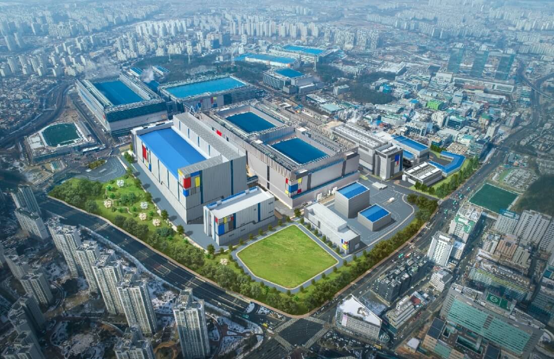
Samsung on Friday announced it has broken ground on a new EUV (extreme ultraviolet) manufacturing facility in Hwaseong, South Korea. The $6 billion project is expected to be completed by the second half of 2019 ahead of production ramp-up in 2020.
The state-of-the-art fabrication facility will be set up with EUV lithography equipment capable of overcoming nano-level technology limitations. Samsung will initially focus on 7-nanometer (nm) LPP (Low Power Plus) EUV process technology.
Just yesterday, we learned that Qualcomm will utilize Samsung’s 7nm process to manufacture future Snapdragon 5G mobile chipsets. And it’s not just traditional mobile devices that will benefit – Samsung anticipates the facility helping to strengthen its leadership in multiple areas including networking, servers, mobile and high-performance computing.
Compared to Samsung’s 10nm FinFET process, the new 7nm EUV technology allows up to a 40 percent increase in area efficiency which customers can tweak for up to 30 percent lower power consumption or 10 percent higher performance.
Kinam Kim, President and CEO of Device Solutions at Samsung Electronics, said that with the addition of the new EUV line, Hwaseong will become the center of the company’s semiconductor cluster spanning Giheung, Hwaseong and Pyeongtaek.
https://www.techspot.com/news/73426-samsung-breaks-ground-new-euv-manufacturing-facility-south.html
