Samsung shares 1,000-layer V-NAND and GDDR7 plans during annual tech conference

Shawn Knight

Posts: 15,294   +192
Staff member
What just happened? Samsung at its annual Tech Day conference in San Jose unveiled its fifth-gen 10nm-class (1b) DRAM as well as eighth- and ninth-generation Vertical NAND (V-NAND) tech. The new 1b DRAM is expected to enter mass production in 2023, but Samsung is already hard at work trying to overcome challenges in scaling beyond 10nm.

It believes disruptive solutions in patterning, architecture and materials will be instrumental in shrinking the process even further, with one example of forward-looking tech being High-K material that is already in development.

Samsung has been iterating its V-NAND tech for a decade and has progressed through several generations. The juice is no doubt worth the squeeze as Samsung has realized 10 times the layer count and 15 times the bit growth through eight generations.

The company's 1Tb TLC V-NAND will be available to customers by the end of the year and work is already under way on ninth-gen V-NAND slated for mass production in 2024. By 2030, Samsung expects to be able to stack over 1,000 layers in its V-NAND.

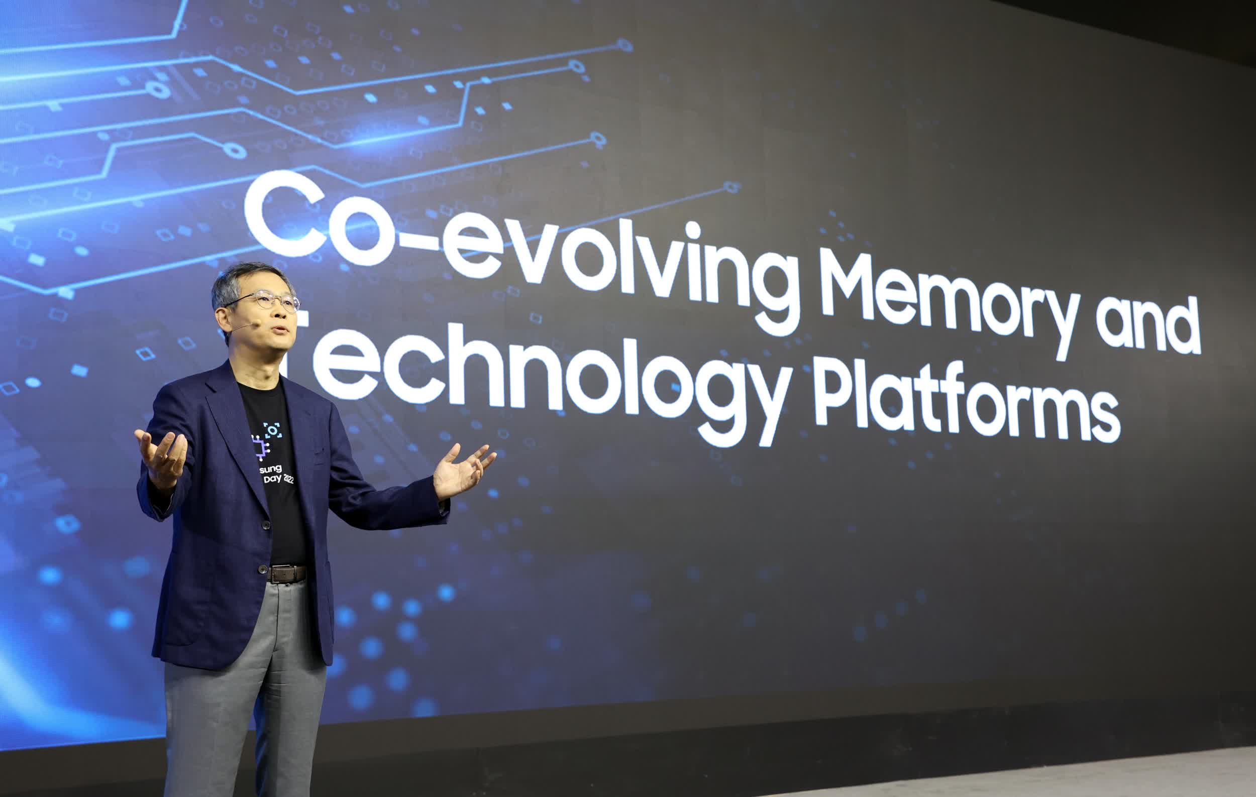
Samsung Tech Day has been held annually since 2017. This year's conference marked the return of in-person attendance following the pandemic. According to Samsung, more than 800 customers and partners attended the one-day event at the Hilton San Jose hotel.

The hardware maker is also accelerating its transition to quad-level cell (QLC) flash while simultaneously enhancing power efficiency. Samsung said this advancement will specifically aid those working with artificial intelligence and big data applications.

Samsung also briefly touched on its GDDR7 DRAM. At 36Gbps, the data rate is double that of GDDR6 and could help to deliver significantly more bandwidth to beefy GPUs set to roll off assembly lines in the not-too-distant future.

Jung-bae Lee, who leads Samsung's memory business, said the company has produced one trillion gigabytes of memory over the last 40+ years. Remarkably, about half of that capacity was manufactured in the last three years alone, highlighting the unprecedented demand as our digital evolution continues.

Permalink to story.

 
So I guess HBM has been designated to cache status...
Nvidia's H100 SXM5 uses Samsung HBM3 modules, which are 1024 bits wide. Although there are six modules on the board, one is redundant, so the 5 modules in use give a bus width of 5120 bits. Even at 3 Gbps, a LOT slower than GDDR7, that's still 1.875 TB/s of bandwidth.

Assuming GDDR7 modules are still 32 bits in width, a GPU with a 384 bit width memory bus would need modules running at 40 Gbps to match that. Now Samsung's claims of 36 Gbps is pretty close, so it would seem that HBM is indeed useless.

However, it's about using it in the more appropriate scenario. GDDR7 is essentially fast-but-narrow, whereas HBM is slow-but-wide.each memory controller can only transfer 32 bits per cycle; a HBM3 MC can do 1024.

If the application requires a shed load of data per cycle (e.g. big data analysis), then HBM3 is the way to go. On the other hand, 3D graphics rendering is working on 32 bits at a time, which is why GDDR is still the preferred choice of DRAM for graphics cards.
 
2030, sure let's announce tech 8 years away as though we care.
This reminds me of back when Intel's Pentium was hitting 3GHz and Intel revealed a "roadmap" where they would be scaling speed quickly to 10GHz in a number of years. How did that work out?
 
This reminds me of back when Intel's Pentium was hitting 3GHz and Intel revealed a "roadmap" where they would be scaling speed quickly to 10GHz in a number of years. How did that work out?
Intel's "road maps", are at best, overly optimistic half truths, but more often outright, bold faced lies, constructed to blow billowing clouds of sunshine and lavender up their stockholders a**es.

While I do build with Intel CPUs, years ago I put my foot down, swearing not to buy another one, until they offered a 10 nm, (or narrower) part.

Not wanting to go back on my oath to myself, I did buy a 12th generation i3-12100. But as my "latest" CPU is an i5-6600K, that purchase was at least 5 years in the making.

The i5 w/board (Gigabyte Z170 Matx w 4 DIMM slots) retailed @ about $80.00) cost me $220.00, at the crossover to 7th generation's introduction.-

No, I didn't buy a "K" CPU to overclock it. I bought it so I didn't have to bother throwing away another Intel stock cooler.
 
Last edited:
Back