Forward-looking: TSMC and Samsung have been attempting to leapfrog one another in terms of extreme ultraviolet lithography. After years of waiting, it seems the industry is finally making strides with EUV, as TSMC announced it also has a 6nm process shrink set to go into risk production.
TSMC doesn't want to be left out of the conversation as it pertains to semiconductors at 6nm. Trailing news of Samsung's progress in the realm of 5nm and 6nm process nodes, TSMC announced its N6 process, based on 6nm EUV.
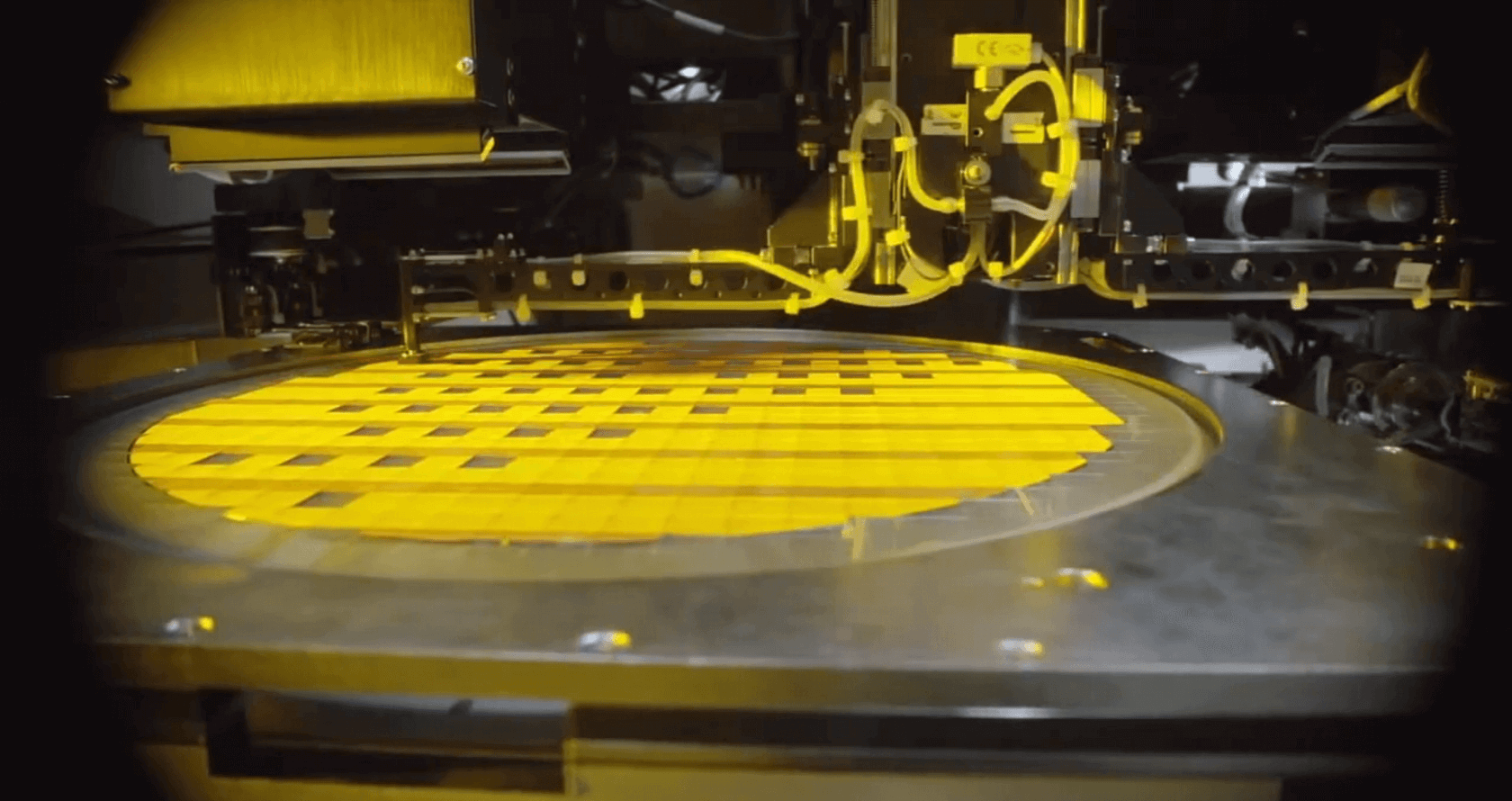
TSMC's 6nm manufacturing process is largely a migration from its 7nm N7 process that sees much of the IP and development ecosystem recycled, so to speak. TSMC is able to take what it has learned with EUV at 7nm and port it directly down to 6nm, keeping the same design rules compatible and speeding up the time to market. This also makes it easier for customers to get started on the process.
By keeping the same design rules, previous N7 customers are able to leverage the N6 process at considerable cost savings, while enjoying what TSMC states is around a 15 percent die shrink. Furthermore, the N6 process is supposed to deliver an 18 percent increase in transistor density while maintaining the same performance and power consumption enhancements.
TSMC is expecting the N6 process to be adopted for applications in mobile, consumer applications, AI, networking, 5G infrastructure, GPU, and high-performance computing.
Risk production is scheduled for the first quarter of 2020; volume production likely won't be until 2021. While TSMC's progress with EUV is considerable, it'll be interesting to see what customers might be interested in such an intermediary node.
https://www.techspot.com/news/79696-tsmc-reveals-n6-process-based-6nm-euv.html
