In context: The migration towards ever-shrinking transistors continues unabated. While Intel is still trying to propel itself over the 10nm hurdle, Samsung and others are looking towards 5nm, 6nm, and even 3nm. Samsung has completed process development for its 5nm EUV node, and the technology is expected to power new applications in 5G, artificial intelligence, high-performance computing and automotive.
It's widely been forecast that Samsung will cede the coveted semiconductor crown to Intel in light of the DRAM market trending downwards. Even Gartner as said as much recently.
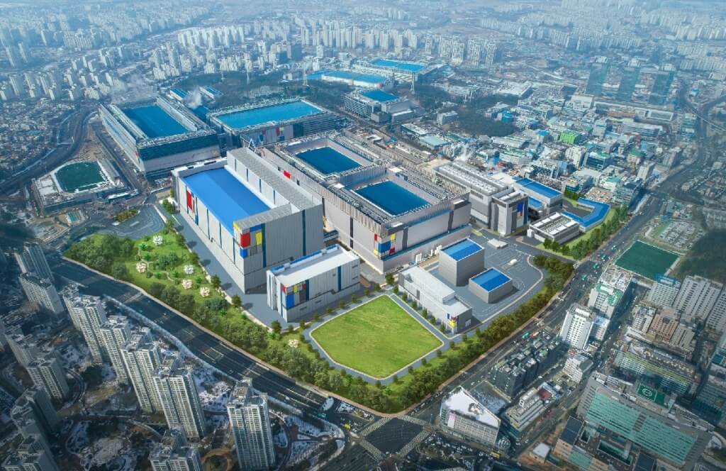
That said, Samsung can't afford to sit idle; rather, it is investing in a slew of new technology to grow and gain a competitive advantage when the memory market rebounds. For instance, the company has announced its new HBM2E memory and the doubling of an investment in EUV at its Hwaseong plant. In fact, it would seem Samsung's continued investment in extreme ultraviolet lithography bears fruit.
Samsung's 7nm 7LPP process has been in mass production since October 2018, and now the company is looking forward to 5nm and beyond. To that end, the memory conglomerate has announced the completion of its 5nm FinFET process that leverages EUV technology.
Compared to its 7nm process, Samsung boasts that the 5nm EUV process will bring "up to a 25 percent increase in logic area efficiency with 20 percent lower power consumption or 10 percent higher performance." Samsung also noted the migration from 7nm to 5nm was eased by being able to reuse much of the intellectual property developed for 7nm. TSMC seemed to enjoy a similar benefit when it recently announced its 5nm development progress.
While there's no word on mass production for 5nm or what customers are on tap for designs, Samsung did say 5nm is ready for customer sampling. Samsung is also reportedly taping out designs for 6nm, but was mum on who its customers were.
