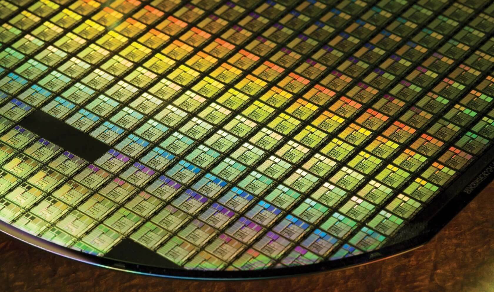
Why it matters: In order to remain competitive and retain its manufacturing leadership, TSMC has to continue to execute on its foundry roadmap. With its 5nm design infrastructure complete and 5nm chips being in risk production, TSMC looks to be in a good position and can look forward to an influx in contracts for 5nm chips. TSMC had previously targeted 5nm volume production for 2020, with 3nm set for 2022.
TSMC has announced that it has completed infrastructure design on its 5nm process node that will leverage the company's second generation of extreme ultraviolet (EUV), as well as deep ultraviolet (DUV) lithography. TSMC's 5nm chips will be aimed at SoC designs, 5G mobile applications, AI, and high performance computing.
According to early numbers on an Arm Cortex-A72 core, TSMC's 5nm process will deliver 1.8 times the density and a 15 percent gain in clock speeds compared to 7nm, and that's based on process refinements alone. TSMC also notes that its second generation of EUV will both simplify the manufacturing process and present excellent yield learning, allowing the process to mature more quickly.
TSMC has also completed development of its 5nm Design Rule Manual (DRM), SPICE model (simulation program with integrated circuit emphasis), and process design kits (PDK). The entirety of the 5nm design infrastructure is available for TSMC customers via TSMC Online. TSMC also notes it has chips in risk production with its alpha customers, which likely indicates volume production could ramp in 2020. That would align with TSMC's previous plans to hit 5nm by 2020 and 3nm by 2022.
TSMC continues to maintain process prowess and leadership, and earning a lot of chip contracts as such. Meanwhile, a lot of companies have seemingly lost faith in Intel, the once market leader.
