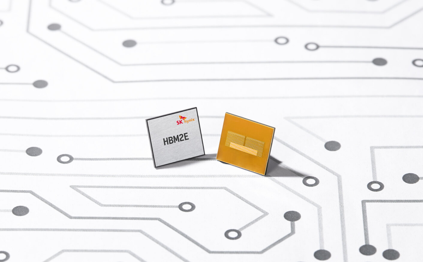
Something to look forward to: To meet growing industry demands for increased performance, SK Hynix, one of the well-known names in DRAM manufacturing, besides Samsung, has announced HBM2E-based DRAM which it says will be faster than its Korean counterpart. While no clear date was given by Samsung on when it'll bring its Flashbolt chips to market, SK Hynix is expecting its product to begin mass production in 2020.
Hot on the heels of Samsung and its "Flashbolt" HBM2E memory, SK Hynix has now become the second DRAM manufacturer to announce its next-gen HBM2E that boast 3.6Gbps (vs 3.2Gbps of Samsung's Flashbolt) speed performance per pin with 1,024 data I/Os.
Offering a 50 percent jump over previous-gen HBM2, the next-gen HBM2E also has "100% additional capacity" according to SK Hynix. By vertically stacking eight 16-gigabit chips, packages of 16GB solutions will be possible through utilization of TSV (Through-silicon via) technique. For advanced hardware employing multiple stacks like server GPUs, 4-stack processors could be paired up with as much as 1.84TB/sec of memory bandwidth.
SK Hynix is aiming its DRAM at "high-end GPU, supercomputers, machine learning, and artificial intelligence systems that require the maximum level of memory performance," which the company says allows for faster data transfer owing to the HBM interface that results in the DRAM sitting ㎛ units apart from GPUs and logic chips as opposed to commodity DRAM products that take the shape of module packages and are mounted on system boards.
"SK Hynix has established its technological leadership since its world's first HBM release in 2013," said Jun-Hyun Chun, Head of HBM Business Strategy.
