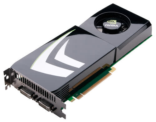
Nvidia GeForce GTX 275
| GPU Snapshot | |||
| Release date: | Jan 15, 2009 | Price at Launch: | $249 |
| Type: | Desktop | Architecture: | Tesla |
| Generation: | GeForce GTX 200 series | Product Tier: | High-end |
| VRAM Capacity: | 0.896 GB | Total Board Power: | 219 W |
| Core Configuration | |||
| Shader Cores: | 240 | TMUs: | 80 |
| ROPs: | 28 | L2 Cache: | 224 KB |
| Memory | |||
| VRAM Capacity: | 0.896 GB | Memory Type: | GDDR3 |
| Memory Speed: | 2.268 Gbps | Memory Bus: | 448-bit |
| Bandwidth: | 127.4 GB/s | ||
| Graphics Processing | |||
| Base Clock: | 633 MHz | FP32 Throughput: | 0.674 TFLOPs |
| Ray Tracing: | No | Process Size: | 55nm |
| Process Name: | TSMC 55nm | Die Size: | 470 mm² |
| Power & Connectivity | |||
| Total Board Power: | 219 W | Power Connectors: | 2x 6-pin |
| Bus Interface: | PCIe 2.0 x16 | DSC: | No |
| Max Displays: | 2 | ||
| Media & Software Support | |||
| DirectX Support: | 11.1 | Shader Model: | 4.0 |
| OpenGL Version: | 3.3 | ||
Reviews and Ratings
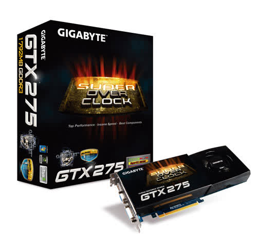
Gigabyte GTX 275 SOCAs we stated in the introduction to this review there are really only two ways for manufacturers to approach GeForce sales in the current market. It has to be value or performance and Gigabyte aimed for the latter with their GTX...
By HardwareHeaven onGigabyte GV-N275SO (GeForce GTX 275 SuperOverclock) 1792MB is a very interesting product. Our tests prove that the card can outperform even the more expensive GTX 285. Plus a certain stepping stone for future models, as this huge memory capacity is...
By iXBT Labs onReviewing a product such as the GTX 275 Super Overclock really isn’t easy since it’s one of those cards that could have been a market leader if its release was just timed right. Gigabyte overclocked this thing to unbelievable heights and its...
By Hardware Canucks onA estas alturas resulta un tanto difícil evaluar una tarjetas como es una GeForce GTX 275, puesto que son tarjetas realmente difíciles de encontrar y aunque demos con ellas normalmente resultan demasiado caras para lo que ofrecen. Es mejor ir...
Même si tous les yeux sont tournés vers les Radeon HD 5000, Gigabyte nous propose avec sa GeForce GTX 275 Super Overclock une très bonne carte graphique. Sur son site, le fabricant annonce des performances en hausse de 9% par...
The GIGABYTE Super Overclock 275GTX video card performance during the non Physx testing portion ranges from 5% to 25% increase on average frame rate scores. During the Physx testing portion I was getting anywhere from 5% to 11% increases during the...
By Bjorn3D on