Nvidia GeForce GTX 465



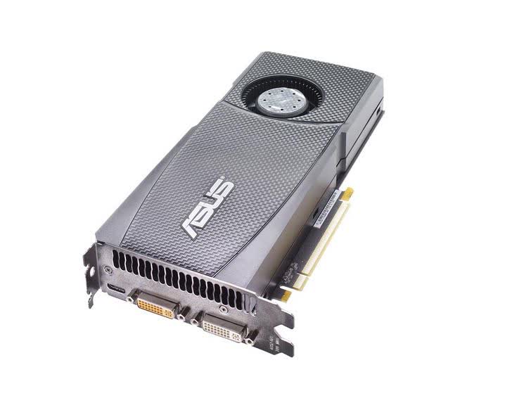
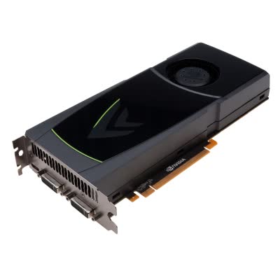
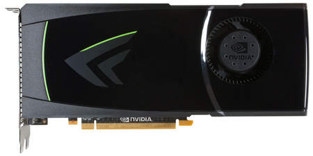
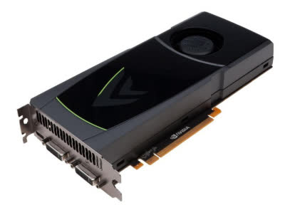
| GPU Snapshot | |||
| Release date: | May 31, 2010 | Price at Launch: | $279 |
| Type: | Desktop | Architecture: | Fermi |
| Generation: | GeForce GTX 400 series | Product Tier: | Midrange |
| VRAM Capacity: | 1 GB | Total Board Power: | 200 W |
| Core Configuration | |||
| Shader Cores: | 352 | TMUs: | 44 |
| ROPs: | 32 | L2 Cache: | 512 KB |
| Memory | |||
| VRAM Capacity: | 1 GB | Memory Type: | GDDR5 |
| Memory Speed: | 3.2 Gbps | Memory Bus: | 256-bit |
| Bandwidth: | 102.7 GB/s | ||
| Graphics Processing | |||
| Base Clock: | 608 MHz | FP32 Throughput: | 0.855 TFLOPs |
| Ray Tracing: | No | Process Size: | 40nm |
| Process Name: | TSMC 40nm | Die Size: | 529 mm² |
| Power & Connectivity | |||
| Total Board Power: | 200 W | Power Connectors: | 2x 6-pin |
| Bus Interface: | PCIe 2.0 x16 | HDMI Support: | HDMI 1.3a |
| DSC: | No | Max Displays: | 2 |
| Media & Software Support | |||
| DirectX Support: | 12 | Shader Model: | 5.1 |
| OpenGL Version: | 4.6 | ||
Reviews and Ratings
Reviewers Liked
- High minimal performance, High performance with enabled tessellation, Wide range of supported FSAA modes, Improved CSAA/TMAA quality, Minimal effect of FSAA on performance, DirectX 11, Shader Model 5.0 and DirectCompute 11 support, CUDA and PhysX support
Reviewers Didn't Like
- Low performance for its price segment, Yields to GeForce GTX 275 in a number of cases, Insufficient performance of the TMU subsystem, Low memory subsystem bandwidth, High power consumption, High noise, Tendency to overheat, Modest overclocking potential
An improvement over the first Fermi cards, but not enough of one to worry ATI...
By PC Pro onPutting together these value comparisons is harder than it looks. Oh, sure, looking at our overall value graphs and making broad generalizations is a lot of fun, but it can be quite misleading. You've gotta keep the hidden variables in mind. If this...
By The Tech Report onThe GeForce GTX 400 series was expected to expand, just like any other new generation of graphics cards. But as opposed to AMD that had no problems spreading its Radeon HD 5000 architecture into all price segments, Nvidia’s promotion of GeForce...
By X-bit Labs onPas sûr que la GeForce GTX 465 puisse trouver son public. Dominée par sa concurrente directe dans les jeux et dans la consommation électrique, elle n'arrive à se rattraper qu'avec la panoplie de technologies tierces NVIDIA...
 By Les Numériques
on
By Les Numériques
on
Enfin, notre choix entre les deux, logiquement on devrait vous conseiller les GTX 465, si la politique tarifaire était respectée, mais les nombreuses promos sur la GTX 470 et les problèmes de distribution de la GTX 465 nous font dire...
By CowcotLand
on
Die GeForce GTX 480 darf sich mit dem Titel der schnellsten (und stromdurstigsten) Einzel-GPU-Karte schmücken. Heute stellt Nvidia mit der GeForce GTX 465 ein Derivat vor, das auf dem gleichen riesigen GF100-Chip basiert. Wenn man es genau nimmt,...
By Tom's Hardware
on
Während AMD bereits in allen Preisbereichen attraktive DirectX-11-Grafikkarten anbietet, kämpft sich Nvidia langsam in niedrigere Preissegmente vor. Auf die Geforce GTX 480 () und Geforce GTX 470 () folgt die GTX 465 zu einer unverbindlichen...
By PC Games Hardware
on
It's not certain that the GeForce GTX 465 will find a big customer base. Dominated by the Radeon HD 5850 in gaming and in terms of economy of energy, it will only make up any ground though the popularity of third party NVIDIA technology (3D Vision...
By DigitalVersus on