And now, for some context
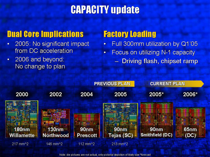
In the early 2000s, Intel's desktop roadmap was defined by one overarching ambition: ever-higher clock speeds. This became known as the "GHz race," a period when raw clock speed was the most visible (and marketable) measure of CPU performance. Riding the momentum of the NetBurst microarchitecture, the company planned an aggressive successor to the Pentium 4 Prescott. That successor was code-named Tejas, with Jayhawk positioned as its server-class counterpart under the Xeon brand.
Intel officially unveiled the Tejas design in early 2003, and the headline target was bold even by the standards of the clock-speed wars: launch frequencies of 7 GHz or more.
At a time when mainstream CPUs were just crossing the 3 GHz mark, this projection captured the imagination of enthusiasts and analysts alike. The assumption was simple: longer pipelines, higher frequencies, and improved manufacturing would keep NetBurst scaling well into the mid-2000s.
Reality intervened quickly.
Tejas was delayed from an expected 2004 debut to sometime in 2005, and internal test silicon revealed the cracks in the strategy. An early 90 nm Tejas sample using LGA 775 reportedly carried a 150 W TDP at only 2.8 GHz, a staggering figure.
For comparison, a 90 nm Prescott-based Pentium 4 at the same frequency sat around 84 W, while the upcoming 65 nm Core 2 Duo would later top out at 65 W even at 3 GHz. Heat density and power delivery were becoming unmanageable, especially for desktops and servers.
By May 2004, Intel cancelled both Tejas and Jayhawk outright, effectively ending NetBurst's future. The company pivoted instead to efficiency-focused designs derived from its mobile architectures, culminating in Core.