
Something to look forward to: Why has Intel chosen to make the huge strategic pivot and investment to not only make chips for itself – as it's always done – but open up their factories to manufacture chips for other companies? It's a particularly vexing question for the company because they did try the chip foundry model – building chips for other companies – and it failed on two previous occasions.
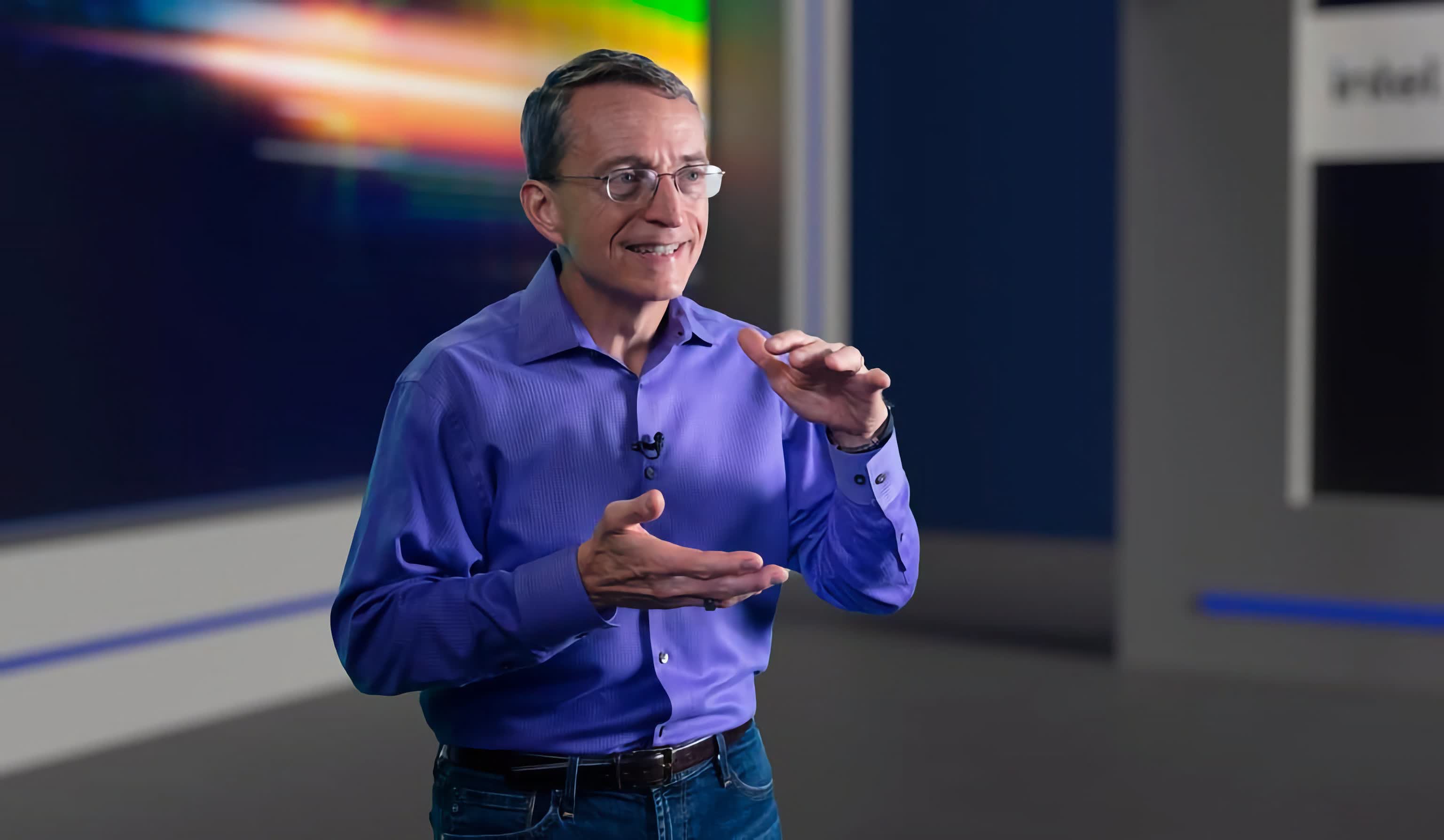
In advance of the company's first event dedicated to their Intel Foundry business happening this week called IFS Direct Connect, I had the opportunity to sit down one-on-one with Intel CEO Pat Gelsinger to get a sense of what his and the company's strategic goals are in making this bold move.
It turns out packaging technology – which enables the combining and interconnecting of multiple smaller chiplets into larger, more sophisticated SoCs – is a key part of it. As Gelsinger related, "[We're doing] proper wafer on wafer level assembly technologies with very advanced capabilities. We've been working in these areas for decades and our leadership here is all of a sudden very interesting."
Based on the impressive array of speakers that Intel has scheduled for the event, including Microsoft CEO Satya Nadella, Arm CEO Rene Haas, OpenAI CEO Sam Altman, US Secretary of Commerce Gina Raimondo, and executives from MediaTek, Broadcom, UMC, Cadence, Synopsys and more, there's clear industry excitement around the new resources that the Intel Foundry is bringing to market. There were even hints of some potential surprises coming out of IFS Direct Connect.
Intel and Gelsinger refer to these kinds of capabilities as a system-level foundry. The idea is that in a world of increasingly sophisticated chip designs, it takes a lot more than the latest and smallest process technologies to put together the most sophisticated and most powerful semiconductors.
"What we found was everybody needed advanced packaging," Gelsinger said, "so instead of this just being something that we can do, it's become a foundational offering."
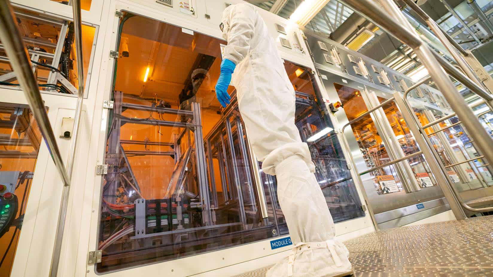
Of course, Intel has made progress on the traditional process advancements. The company is expected to discuss the state of the aggressive "5 nodes in 4 years" (5N4Y) initiative it started two years ago at this week's event. The critical role of packaging, interconnect and other elements that allow the creation of "systems of chips," however, is where the company offers some unique advantages and some important opportunities.

"Why can't Nvidia today do 2X the number of GPUs the world wants?," Gelsinger opined. "It's not because of silicon, it's because of packaging."
In the case of advanced AI accelerator chips that the world is likely going to need large quantities of soon, some of these packaging capabilities and this system-level thinking are going to be particularly important Gelsinger said.
"The AI chips of the future will have multilayer 3D packaging with cache and memory arrays and chiplets on top," he noted. "I probably want to connect those chiplets together with some form of UCIe through some hybrid bonding or something like that onto a base chip as well," he continued. "I [also] need to have all of the drivers, the base level capabilities associated with that software to compose this thing. These are just some of the examples of what it takes to be that next generation system foundry."
Inherent in Gelsinger's comments is the company's willingness to share both IP and expertise it has developed in creating its own chips with foundry customers. "Our client designs were doing this [advanced package design] already and we're making that expertise of how to compose these fully available as part of the foundry service offerings."
That's part of the changes that Gelsinger has made in this latest attempt to build a foundry business inside Intel. In addition, the company has done work to integrate much more easily with the entire chip design industry, particularly with EDA software companies like Cadence and Synopsys. "In the past, Intel was always super proprietary," Gelsinger said. "You had to jump over this huge amount of effort [to learn] all of our proprietary tools and flows. That's why the Cadence and Synopsys relationships are so important."
While Gelsinger freely admitted that it was still too early to tell, he did suggest that the approaches they're taking and the emphasis on packaging and systems design they have are moving them past earlier foundry efforts. "We've said we're over $10 billion in lifetime deal value and that's multiples of what it was in the past. We're also way past the amount of revenue, customers, etc., that was ever part of those earlier efforts."
In addition to the practical demand and design requirements for advanced packaging technologies, Gelsinger also pointed out how the economics of modern chip design and manufacturing are evolving.
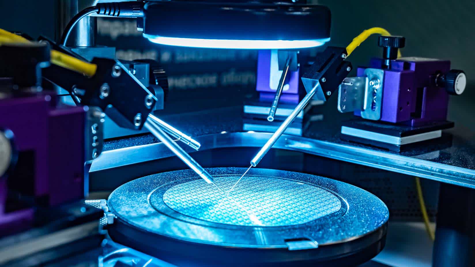
"If we would go back five years for a leading-edge CPU, in the Bill of Materials, 15% [of the cost] would be for package assembly and test. As we get to one of the modern chips, like Gaudi [an Intel AI Accelerator chip] or Granite Rapids [a future Intel server CPU], that are using these 3D construction technologies, package assembly and test is now 35 to 40%. So, the total value of the product is becoming much more, seen through the package assembly and test layers."
Of course, another reason the company is pursuing this foundry model is due to both the surprising lack of geographical manufacturing diversity in the chip business and the stark reality of today's geopolitical environment.
At present, over 50% of all the world's semiconductors and about 90% of the most advanced chips are built in Taiwan by TSMC, USMC and others. The problem is that China has recently been raising several red flags hinting at a potential invasion and takeover of Taiwan, a country that it believes is still part of China. On top of that, Taiwan sits along the infamous Ring of Fire, a tectonic belt surrounding much of the Pacific Ocean that is known for the kind of earthquake activity that could wreak havoc on the country's infrastructure.
The net result has been a wakeup call heard around the world about the tremendously important need to geographically diversify where chips are made. Long-time semiconductor industry observers have been making this point for decades, but the chip shortages in products like cars that happened during the pandemic shone an intense new light on the problem.
As a result, governments have started to create huge programs to financially support domestic chip manufacturing activity – including the $52 billion CHIPS Act here in the US, which has just started to dole out its first funds.
Not surprisingly, Gelsinger wants to take advantage of these funds not just because of the obvious economic windfall but because of the need to get the US, Europe, and other parts of the world in a stronger position from a chip manufacturing perspective. "[Asian] governments heavily subsidized [the semiconductor industry] for three decades, and now we're 80% dependent on Asia," he said. "If we're going to bring it back, we have to close the economic gap, right?"
Unfortunately, the process of getting those funds has proven to be slower than expected. Gelsinger commented, "When I stood on the White House lawn at the signing of the bill in August of 2022, did I think I'd be sitting here talking to you today, and say, I haven't seen a penny yet? No." Those funds are critical too because as Gelsinger pointed out, "We're making investments with the presumption that these grants, tax credits, etc., materialize."
In the end, Gelsinger is positive about the efforts, but time is of the essence. "I feel like I have a commitment from Congress here and a commitment from Parliament and the EU, but you know, at some point the [Intel] board's gonna say, OK, Pat, enough's, enough."
Government subsidies aside, it takes a lot more than opportunism to build a successful foundry business and Gelsinger knows it.
Intel can't make a serious run at it without having the kinds of chip manufacturing competencies that other companies want to use. Ultimately, it's those unique capabilities in packaging and chip systems design, as well as a purpose-driven approach that will make or break the audacious plan upon which Gelsinger and Intel have embarked.
It's clearly not an easy goal, but it is one he seems driven to achieve.
Bob O'Donnell is the founder and chief analyst of TECHnalysis Research, LLC a technology consulting firm that provides strategic consulting and market research services to the technology industry and professional financial community. You can follow him on X @bobodtech