Every single CPU found in any computer, from a cheap laptop to a million-dollar server, will have something called cache. It must be important, otherwise why would it be there? But what does cache do?
Every single CPU found in any computer, from a cheap laptop to a million-dollar server, will have something called cache. It must be important, otherwise why would it be there? But what does cache do?
The key to overcoming latency with cache (or any computing structure, for that matter) is hiding it underneath other parallel processes. The average access-to-use time for the various levels is non-linear: in Zen 2, L1 is roughly 5 to 7 cycles, L2 is about 14, and L3 is around 40. L1 and L2 cache is inclusive and private to a particular core, I.e. the contents are exclusive to the logic units in that core only. Only the L3 cache is accessible to other cores, but it's a victim cache, so it only stores data that's released from L2.I want to hear how these layers overcome latency and how AMD’s upcoming unified cache will make the 12 and 16 core designs as fast as the 8 core Matisse CPU’s.
Correct, no one suggested L2 was on the motherboard. Pentium II and Celerons of that era came in a daughterboard.Pentium 2 did NOT have an L2 cache on the motherboard. They were on the processor just not on the die. They were on the cartridge next to the die.
Correct, no one suggested L2 was on the motherboard. Pentium II and Celerons of that era came in a daughterboard.
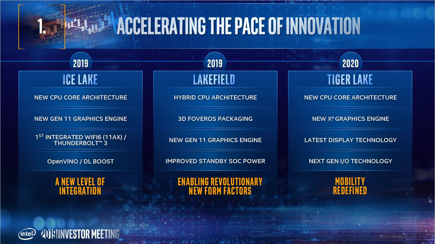
Not much is out in the wilds at the moment. This news report, if showing genuine details on Tiger Lake, suggests some notable changes:Any information on cache expected to show itself in Tiger Lake would be most appreciated too.
It was a shame that Intel dropped it, even though it added a fair bit to the package costs.It had the 128MB of L4 (victim cache) for the Iris GFX. By disabling the Graphics in the BIOS and using a GTX discrete graphics card, that 128MB was used on my audio apps and helped immensely.
Not much is out in the wilds at the moment. This news report, if showing genuine details on Tiger Lake, suggests some notable changes:
Intel "Tiger Lake" Microarchitecture Features HEDT-like Cache Rebalancing?
With its "Skylake" microarchitecture, Intel significantly re-balanced the cache hierarchy of its HEDT and enterprise multi-core processors to equip CPU cores with larger amounts of faster L2 caches, and lesser amounts on slower shared L3 cache. The company retained its traditional cache balance...www.techpowerup.com
Compared to Comet Lake, L1 instruction is the same size at 32 kB, but L1 data has increased by 50% to 48 kB. L2 is 1.25 MB, though - 6 times greater. L3 is 12 MB in total, for 4 cores, so that's gone up by 50% too.
It was a shame that Intel dropped it, even though it added a fair bit to the package costs.
Pentium 2 did NOT have an L2 cache on the motherboard. They were on the processor just not on the die. They were on the cartridge next to the die.

Pentium II - Wikipedia
en.wikipedia.org
The chip on the side is the cache.
The original K6-2 had a 64 KB primary cache and a much larger amount of motherboard-mounted cache (usually 512 KB or 1024 KB but varying depending on the choice of the motherboard). The K6-III, with its 256 KB on-die secondary cache, re-purposed the variable-size external cache on the motherboard as the L3 cache. This scheme was termed "TriLevel Cache" by AMD. The L3 cache has a capacity of up to 2 MB.
The key to overcoming latency with cache (or any computing structure, for that matter) is hiding it underneath other parallel processes. The average access-to-use time for the various levels is non-linear: in Zen 2, L1 is roughly 5 to 7 cycles, L2 is about 14, and L3 is around 40. L1 and L2 cache is inclusive and private to a particular core, I.e. the contents are exclusive to the logic units in that core only. Only the L3 cache is accessible to other cores, but it's a victim cache, so it only stores data that's released from L2.
So let's say core #5 wants a particular piece of data - L1 cache is always checked first and if it's there, it gets used. If not, a check of L2 is skipped automatically, and the memory sub-system goes onto to work through L3, RAM, and eventually the main storage. The thread that required the data will be stalled until the information is available, but if SMT is enabled, the core can still be used to process another thread.
The branch predictor and other cache in the core also helps to mitigate this problem, by trying to determine what data is going to be required ahead of time, and holding branches in the cache until its needed and/or the data is ready.
As for unified cache, technically this just means it's not separated in any way (e.g. L1 is split cache, L2 is unified). L3 already is, by this definition, unified as there isn't a data/instruction/constants type of separation.
However, when we talk about Zen 3 and unified cache, this is referring to the fact that in Zen 2, cross-core access to L3 is confined to a CCX - so cores 0 to 3 in CCX 0 can directly access each other's L3; whereas cores 4 to 7 in CCX 1 can't. In order for, say, core 6 to access the L3 in CCX 0, the request has to be managed (along with the data flow), by the I/O processor.
The general expectation for Zen 3 is that either the management of the two CCX's L3 cache will be managed by a system within the CCD, or the chiplet will contain just a single 8 core CCX. Both methods reduce the overall latency, but former will be simpler to implement that the other.
Impossible to answer without knowing what software usage you intend, and whether it tends to be compute-bound or memory-bound.So the question I have is concerning Zen 2. In deciding which cpu to go with. A faster CPU with a smaller L3 or a slower CPU with the larger L3? I was thinking that I would want as large of L3 as I could get.
General purpose. Games, media play, internet, occasional encodes. No scientific, no crypto, or calculating stuff which I imagine would be more gpu bound. I do tend to keep a lot of windows and multiple browser pages up so definitely a memory hog.Impossible to answer without knowing what software usage you intend, and whether it tends to be compute-bound or memory-bound.
BTW, if any editors are reading, this is the first I glanced at the article, and noticed the following error:
"Transistor-based memory takes up a lot more space than DRAM "
DRAM also contains transistors: one per cell, alongside the capacitor the article mentions. SRAM contains from 4 to 6 per cell, which is one of the reasons it's so much more expensive.
That particular sentence was part of this:BTW, if any editors are reading, this is the first I glanced at the article, and noticed the following error:
"Transistor-based memory takes up a lot more space than DRAM "
DRAM also contains transistors: one per cell, alongside the capacitor the article mentions. SRAM contains from 4 to 6 per cell, which is one of the reasons it's so much more expensive.
Thus the statement of “transistor-based’ memory was referring to the context of the method of data storage: capacitors versus transistors.Where DRAM uses microscopic capacitors to store data in the form of electrical charge, SRAM uses transistors to do the same thing and these can work almost as fast as the logic units in a processor (roughly 10 times faster than DRAM).
There is, of course, a drawback to SRAM and once again, it's about space.
Transistor-based memory takes up a lotmore space than DRAM
Yes, but in that context, "transistor-based memory" also includes flash memory, which takes up less space than DRAM. Even excluding that, the implication of the statement is that the reason SRAM consumes more space is because it's "transistor-based". Capacitors are larger than transistors: DRAM's space advantage comes because its cells require 2 components, not 6.Thus the statement of “transistor-based’ memory was referring to the context of the method of data storage: capacitors versus transistors.
The context is entirely that of SRAM - while the use of the word ‘This’ before ‘Transistor-based memory...’ would arguably make this completely transparent, the statement is close enough to remarks about SRAM for it not be a significant enough issue.Yes, but in that context, "transistor-based memory" also includes flash memory, which takes up less space than DRAM. Even excluding that, the implication of the statement is that the reason SRAM consumes more space is because it's "transistor-based". Capacitors are larger than transistors: DRAM's space advantage comes because its cells require 2 components, not 6.
