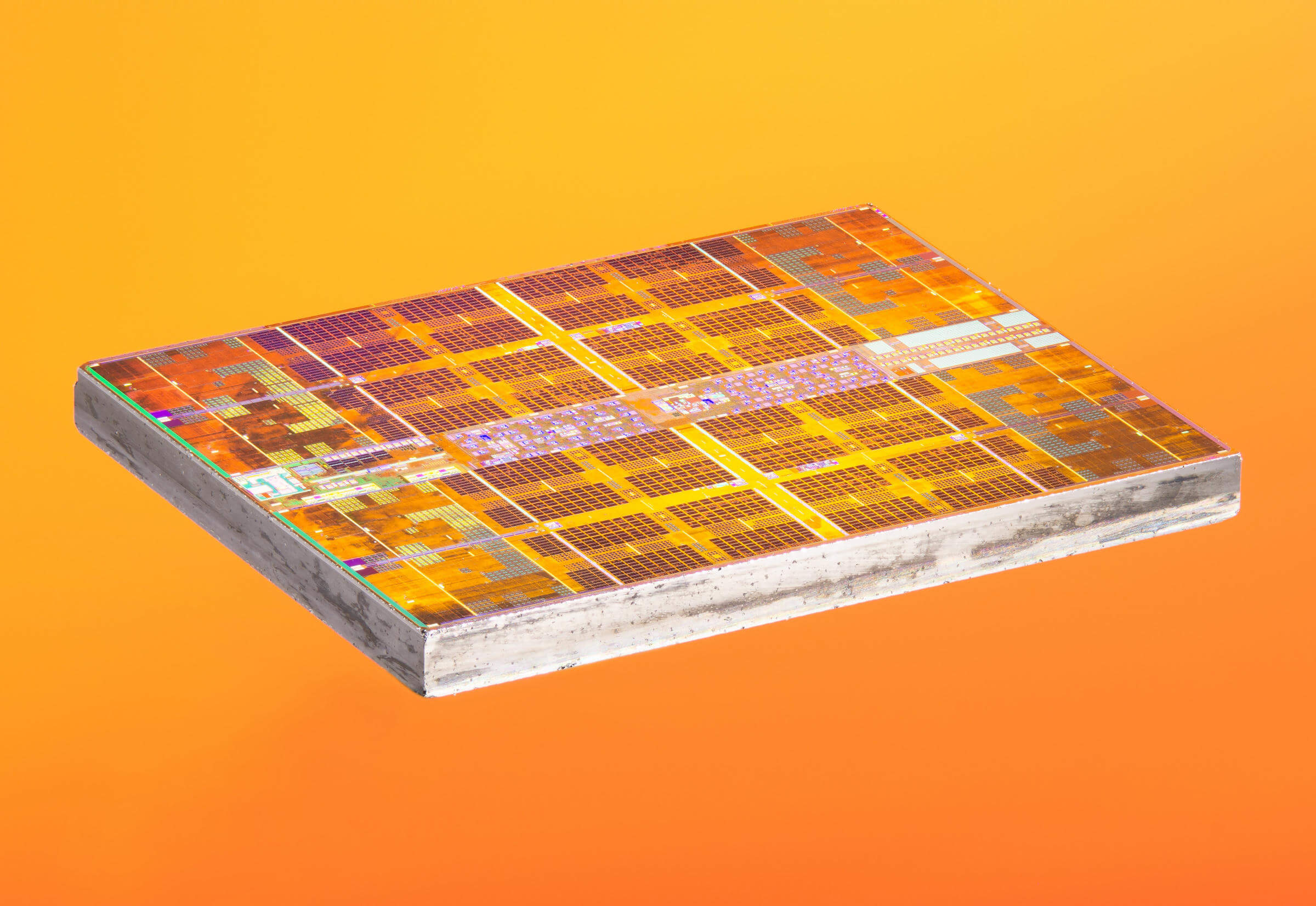
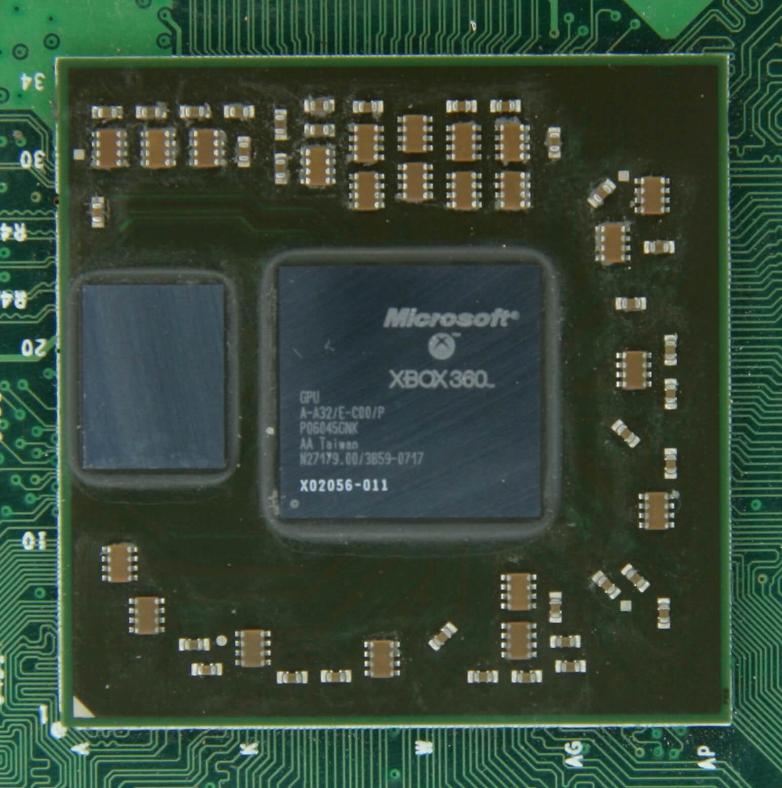
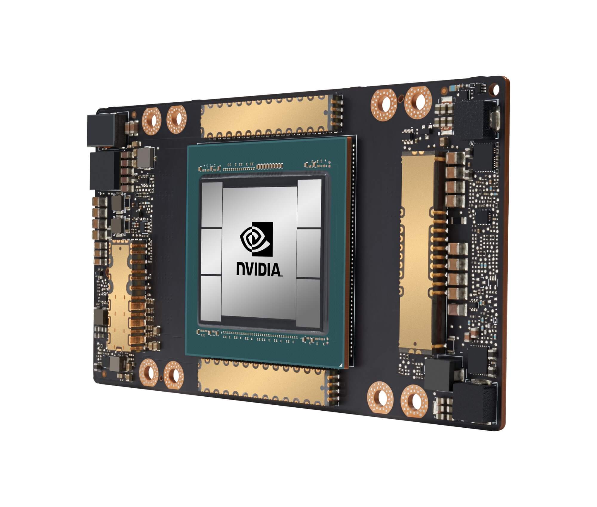
Every single CPU found in any computer, from a cheap laptop to a million-dollar server, will have something called cache. More likely than not, it'll possess several levels of it, too.
It must be important, otherwise why would it be there? But what does cache do, and why the need of different levels of the stuff? What on Earth does 12-way set associative even mean?
What exactly is cache?
TL;DR: It's small, but very fast memory that sits right next to the CPU's logic units.
But of course, there's much more we can learn about cache...
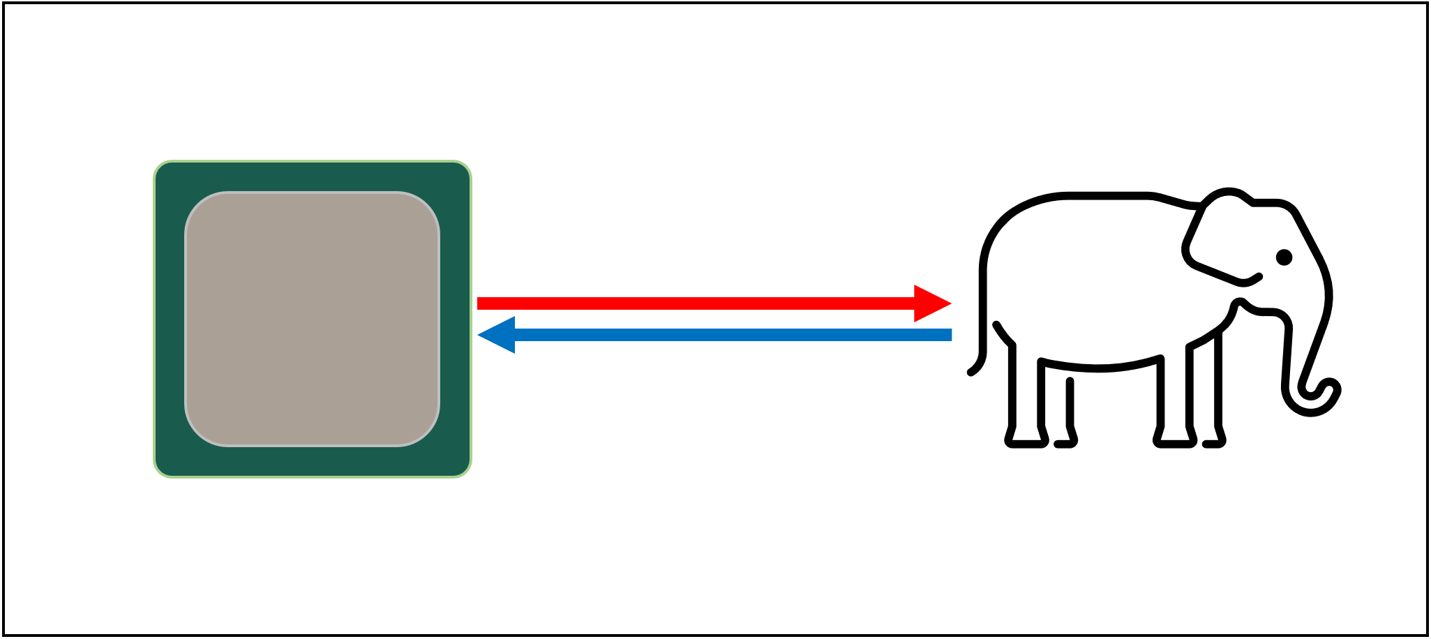
Let's begin with an imaginary, magical storage system: it's infinitely fast, can handle an infinite number of data transactions at once, and always keeps data safe and secure. Not that anything even remotely to this exists, but if it did, processor design would be much simpler.
CPUs would only need to have logic units for adding, multiplying, etc. and a system to handle the data transfers. This is because our theoretical storage system can instantly send and receive all the numbers required; none of the logic units would be held up waiting for a data transaction.
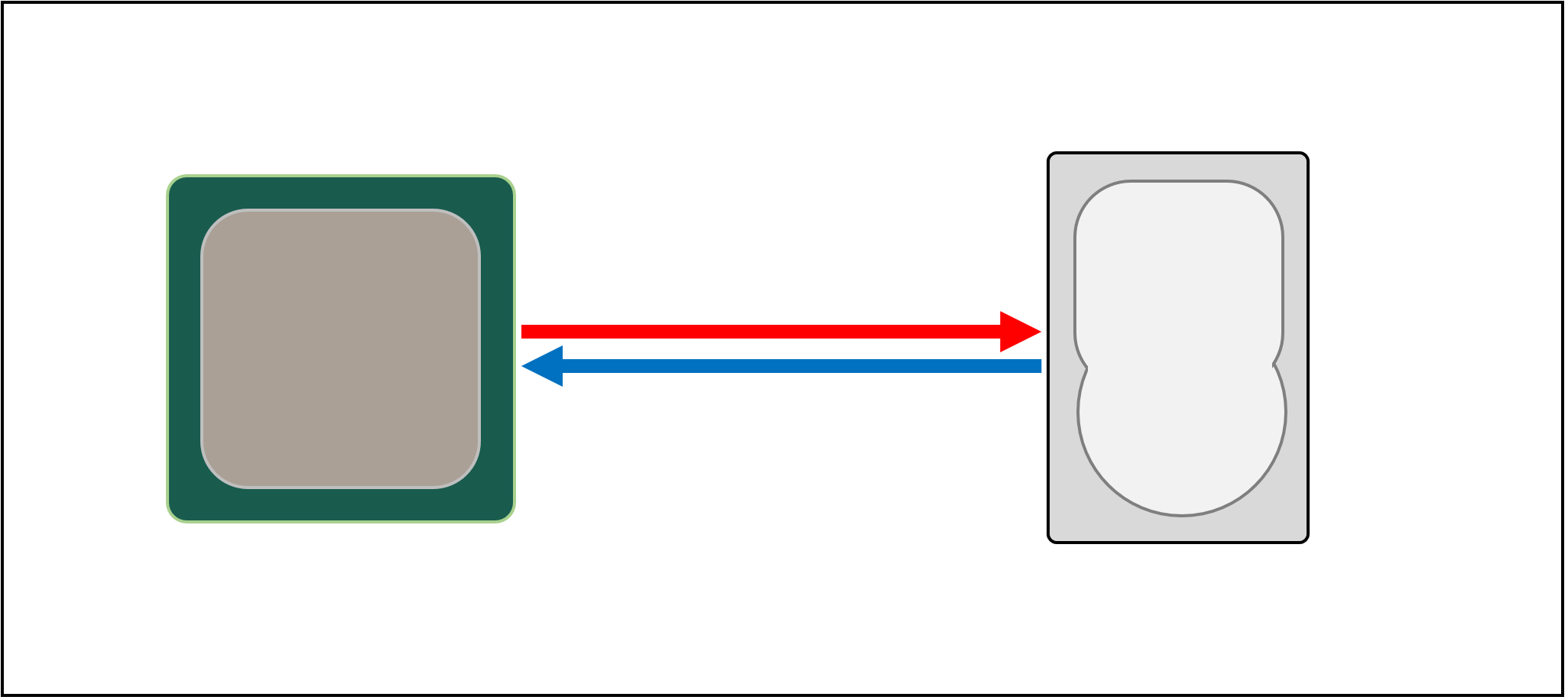
But, as we all know, there isn't any magic storage technology. Instead, we have hard or solid state drives, and even the best of these aren't even remotely capable of handling all the data transfers required for a typical CPU.
The reason why is that modern CPUs are incredibly fast – they take just one clock cycle to add two 64 bit integer values together, and for a CPU running at 4 GHz, this would be just 0.00000000025 seconds or a quarter of a nanosecond.
Meanwhile, spinning hard drives take thousands of nanoseconds just to find data on the discs inside, let alone transfer it, and solid state drives still take tens or hundreds of nanoseconds.
Such drives obviously can't be built into processors, so that means there will be a physical separation between the two. This just adds more time onto the moving of data, making things even worse.
So what we need is another data storage system, that sits in between the processor and the main storage. It needs to be faster than a drive, be able to handle lots of data transfers simultaneously, and be a lot closer to the processor.
Well, we already do have such a thing, and it's called RAM, and every computer system has some for this very purpose.
Almost of all this kind of storage is DRAM (dynamic random access memory) and it's capable of passing data around much faster than any drive.
However, while DRAM is super quick, it can't store anywhere near as much data.
Some of the largest DDR4 memory chips made by Micron, one of the few manufacturers of DRAM, holds 32 Gbits or 4 GB of data; the largest hard drives hold 4,000 times more than this.
So although we've improved the speed of our data network, additional systems – hardware and software – will be required in order to work out what data should be kept in the limited amount of DRAM, ready for the CPU.
At least DRAM can manufactured to be in the chip package (known as embedded DRAM). CPUs are pretty small, though, so you can't stick that much into them.
The vast majority of DRAM is located right next to the processor, plugged into the motherboard, and it's always the closest component to the CPU, in a computer system. And yet, it's still not fast enough...
DRAM still takes around 100 nanoseconds to find data, but at least it can transfer billions of bits every second. Looks like we'll need another stage of memory, to go in-between the processor's units and the DRAM.
Enter stage left: SRAM (static random access memory). Where DRAM uses microscopic capacitors to store data in the form of electrical charge, SRAM uses transistors to do the same thing and these can work almost as fast as the logic units in a processor (roughly 10 times faster than DRAM).
There is, of course, a drawback to SRAM and once again, it's about space.
Transistor-based memory takes up a lot more space than DRAM: for the same size 4 GB DDR4 chip, you'd get less than 100 MB worth of SRAM. But since it's made through same process as creating a CPU, SRAM can be built right inside the processor, as close to the logic units as possible.
Transistor-based memory takes up a lot more space than DRAM: for the same size 4 GB DDR4 chip, you'd get less than 100 MB worth of SRAM.
With each extra stage, we've increased the speed of moving data about, to the cost of how much we can store. We could carry on adding in more sections, with each one being quicker but smaller.
And so we arrive at a more technical definition of what cache is: It's multiple blocks of SRAM, all located inside the processor; they're used to ensure that the logic units are kept as busy as possible, by sending and storing data at super fast speeds. Happy with that? Good – because it's going to get a lot more complicated from here on!
Cache: a multi-level parking lot
As we discussed, cache is needed because there isn't a magical storage system that can keep up with the data demands of the logic units in a processor. Modern CPUs and graphics processors contain a number of SRAM blocks, that are internally organized into a hierarchy – a sequence of caches that are ordered as follows:
In the above image, the CPU is represented by the black dashed rectangle. The ALUs (arithmetic logic units) are at the far left; these are the structures that power the processor, handling the math the chip does. While its technically not cache, the nearest level of memory to the ALUs are the registers (they're grouped together into a register file).
Each one of these holds a single number, such as a 64-bit integer; the value itself might be a piece of data about something, a code for a specific instruction, or the memory address of some other data.
The register file in a desktop CPU is quite small – for example, in Intel's Core i9-9900K, there are two banks of them in each core, and the one for integers contains just 180 64-bit registers. The other register file, for vectors (small arrays of numbers), has 168 256-bit entries. So the total register file for each core is a little under 7 kB. By comparison, the register file in the Streaming Multiprocessors (the GPU's equivalent of a CPU's core) of an Nvidia GeForce RTX 2080 Ti is 256 kB in size.
Registers are SRAM, just like cache, but they're just as fast as the ALUs they serve, pushing data in and out in a single clock cycle. But they're not designed to hold very much data (just a single piece of it), which is why there's always some larger blocks of memory nearby: this is the Level 1 cache.
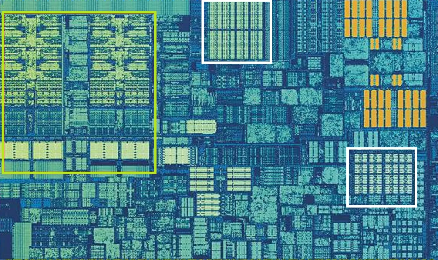
The above image is a zoomed in shot of a single core from Intel's Skylake desktop processor design.
The ALUs and the register files can be seen in the far left, highlighted in green. In the top-middle of the picture, in white, is the Level 1 Data cache. This doesn't hold much information, just 32 kB, but like registers, it's very close to the logic units and runs at the same speed as them.
The other white rectangle indicates the Level 1 Instruction cache, also 32 kB in size. As its name suggests, this stores various commands ready to be split up into smaller, so-called micro operations (usually labelled as μops), for the ALUs to perform. There's a cache for them, too, and you could class it as Level 0, as it's smaller (only holding 1,500 operations) and closer than the L1 caches.
You might be wondering why these blocks of SRAM are so small; why aren't they a megabyte in size? Together, the data and instruction caches take up almost the same amount of space in the chip as the main logic units do, so making them larger would increase the overall size of the die.
But the main reason why they just hold a few kB, is that the time needed to find and retrieve data increases as memory capacity gets bigger. L1 cache needs to be really quick, and so a compromise must be reached, between size and speed – at best, it takes around 5 clock cycles (longer for floating point values) to get the data out of this cache, ready for use.
But if this was the only cache inside a processor, then its performance would hit a sudden wall. This is why they all have another level of memory built into the cores: the Level 2 cache. This is a general block of storage, holding onto instructions and data.
It's always quite a bit larger than Level 1: AMD Zen 2 processors pack up to 512 kB, so the lower level caches can be kept well supplied. This extra size comes at a cost, though, and it takes roughly twice as long to find and transfer the data from this cache, compared to Level 1.
Going back in time, to the days of the original Intel Pentium, Level 2 cache was a separate chip, either on a small plug-in circuit board (like a RAM DIMM) or built into the main motherboard. It eventually worked its way onto the CPU package itself, until being finally integrated into the CPU die, in the likes of the Pentium III and AMD K6-III processors.
This development was soon followed by another level of cache, there to support the other lower levels, and it came about due to the rise of multi-core chips.
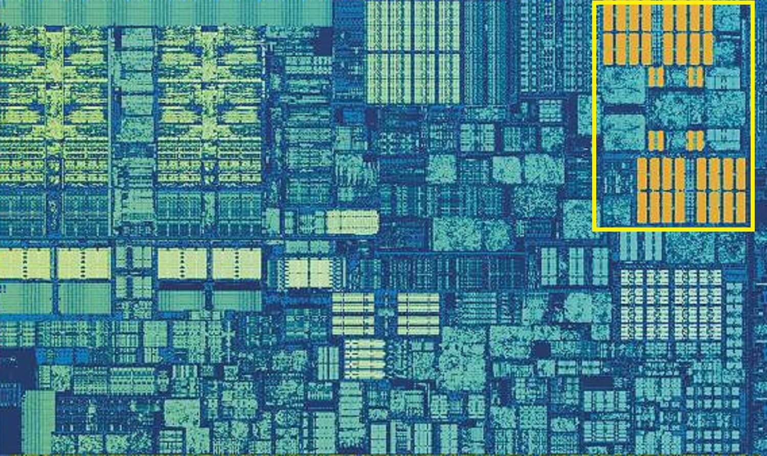
This image, of an Intel Kaby Lake chip, shows 4 cores in the left-middle (an integrated GPU takes up almost half of the die, on the right). Each core has its own 'private' set of Level 1 and 2 caches (white and yellow highlights), but they also come with a third set of SRAM blocks.
Level 3 cache, even though it is directly around a single core, is fully shared with the others – each one can freely access the contents of another's L3 cache. It's much larger (between 2 and 32 MB) but also a lot slower, averaging over 30 cycles, especially if a core needs to use data that's in a block of cache some distance away.
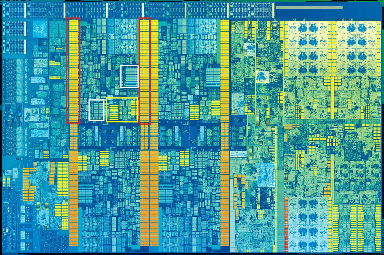
Below, we can see a single core in AMD's Zen 2 architecture: the 32 kB Level 1 data and instruction caches in white, the 512 KB Level 2 in yellow, and an enormous 4 MB block of L3 cache in red.

Wait a second. How can 32 kB take up more physical space than 512 kB? If Level 1 holds so little data, why is it proportionally so much bigger than L2 or L3 cache?
More than just a number
Cache boosts performance by speeding up data transfer to the logic units and keeping a copy of frequently used instructions and data nearby. The information stored in cache is split in two parts: the data itself and the location of where it was originally located in the system memory/storage – this address is called a cache tag.
When the CPU runs an operation that wants to read or write data from/to the memory, it starts by checking the tags in the Level 1 cache. If the required one is present (a cache hit), that data can then be accessed almost straight away. A cache miss occurs when the required tag is not in the lowest cache level.
So a new tag is created in the L1 cache, and the rest of the processor architecture takes over, hunting back through the other cache levels (all the way back to the main storage drive, if necessary) to find the data for that tag. But to make space in the L1 cache for this new tag, something else invariably has to be booted out into the L2.
This results in a near-constant shuffling about of data, all achieved in just a handful of clock cycles. The only way to achieve this is by having a complex structure around the SRAM, to handle the management of the data. Put another way: if a CPU core consisted of just one ALU, then the L1 cache would be much simpler, but since there are dozens of them (many of which will be juggling two threads of instructions), the cache requires multiple connections to keep everything on the move.
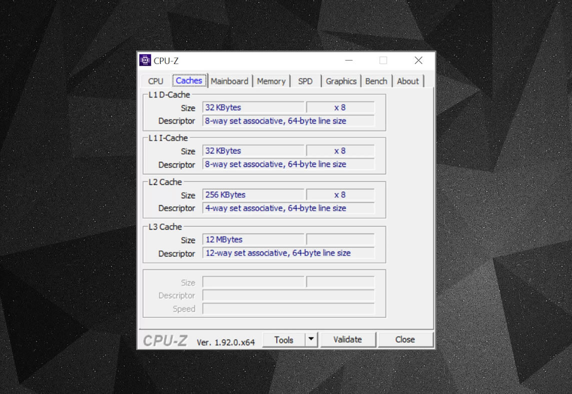
You can use free programs, such as CPU-Z, to check out the cache information for the processor powering your own computer. But what does all of that information mean? An important element is the label set associative – this is all about the rules enforced by how blocks of data from the system memory are copied into the cache.
The above cache information is for an Intel Core i7-9700K. Its Level 1 caches are each split up into 64 little blocks, called sets, and each one of these is further divided into cache lines (64 bytes in size). Set associative means that a block of data from the system memory is mapped onto the cache lines in one particular set, rather than being free to map across anywhere.
The 8-way part tells us that one block can be associated with 8 cache lines in a set. The greater the level of associativity (i.e. more 'ways'), the better the chances of getting a cache hit when the CPU goes hunting for data, and a reduction in the penalties caused by cache misses. The downsides are that it adds more complexity, increased power consumption, and can also decrease performance because there are more cache lines to process for a block of data.
Another aspect to the complexity of cache revolves around how data is kept across the various levels. The rules are set in something called the inclusion policy. For example, Intel Core processors have fully inclusive L1+L3 cache. This means that the same data in Level 1, for example, can also be in Level 3. This might seem like it's wasting valuable cache space, but the advantage is that if the processor gets a miss, when searching for a tag in a lower level, it doesn't need to hunt through the higher level to find it.
In the same processors, the L2 cache is non-inclusive: any data stored there isn't copied to any other level. This saves space, but does result the chip's memory system having to search through L3 (which is always much bigger) to find a missed tag. Victim caches are similar to this, but they're used to stored information that gets pushed out of a lower level – for example, AMD's Zen 2 processors use L3 victim cache that just stores data from L2.
There are other policies for cache, such as when data gets written into cache and the main system memory. These are called write policies and most of today's CPUs use write-back caches; this mean that when data gets written into a cache level, there is a delay before the system memory gets updated with a copy of it. For the most part, this pause runs for as long as the data remains in the cache – only once it's booted out, does the RAM get the information.
For processor designers, choosing the amount, type, and policy of cache is all about balancing the desire for greater processor capability against increased complexity and required die space. If it was possible to have 20 MB, 1000-way fully associative Level 1 caches without the chips becoming the size of Manhattan (and consuming the same kind of power), then we'd all have computers sporting such chips!
The lowest level of caches in today's CPUs haven't changed all that much in the past decade. However, Level 3 cache has continued to grow in size. A decade ago, you could get 12 MB of it, if you were lucky enough to own a $999 Intel i7-980X. For half that amount today, you get 64 MB.
Cache, in a nutshell: absolutely needed, absolutely awesome pieces of technology. We've not looked at other caches types in CPUs and GPUs (such as translation lookup buffers or texture caches), but since they all follow a simple structure and pattern of levels as we've covered here, they perhaps won't sound so complicated.
Did you own a computer that had L2 cache on the motherboard? How about those slot-based Pentium II and Celeron CPUs (e.g. 300a) that came in a daughterboard? Can you remember your first CPU that had shared L3? Let us know in the comments section.
Shopping Shortcuts:
- AMD Ryzen 9 3900X on Amazon
- AMD Ryzen 9 3950X on Amazon
- Intel Core i9-10900K on Amazon
- AMD Ryzen 7 3700X on Amazon
- Intel Core i7-10700K on Amazon
- AMD Ryzen 5 3600 on Amazon
- Intel Core i5-10600K on Amazon
