New Intel research charts a course to trillion-transistor chip designs by 2030

Jimmy2x

Posts: 238   +29
Staff
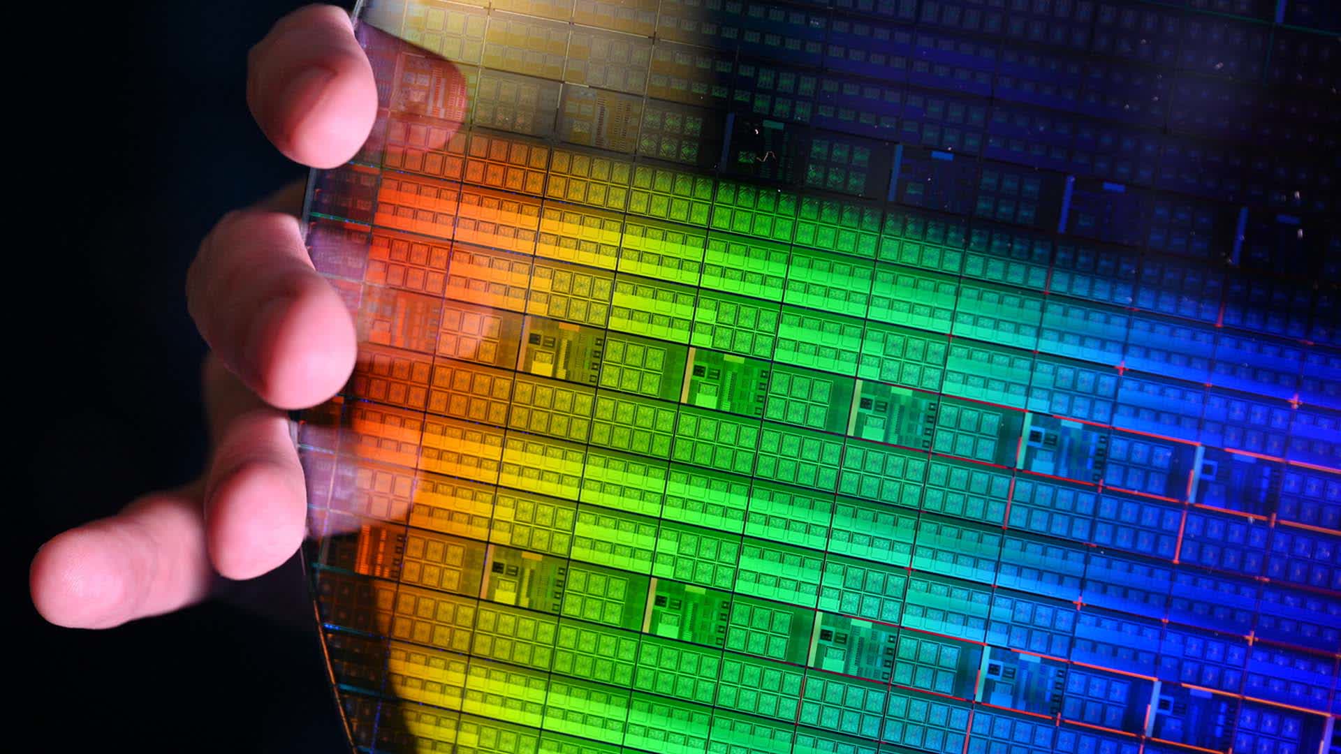
Something to look forward to: Intel submitted several research papers to this year's International Electron Devices Meeting (IEDM), highlighting their plans to pursue new 2D transistor materials and 3D packaging solutions. The new information backs CEO Pat Gelsinger's previous statements regarding Intel's upcoming microarchitecture design innovations. According to Intel's Gary Patton, the new advancements will keep Moore's Law alive and well for the foreseeable future.

Earlier this year, Nvidia's Jensen Huang declared Moore's Law dead (again) during a 4000-series launch Q&A session. The prediction echoed similar statements made by Huang during the 2017 Beijing GPU Technology Conference. And much like those times before, Intel isn't buying what Nvidia's leather leader is selling.

The company's 2023 IEDM research submissions highlight several processes, materials, and technologies that could help the semiconductor giant to support their previous statements on delivering chiplet-based trillion transistor processors by 2030.

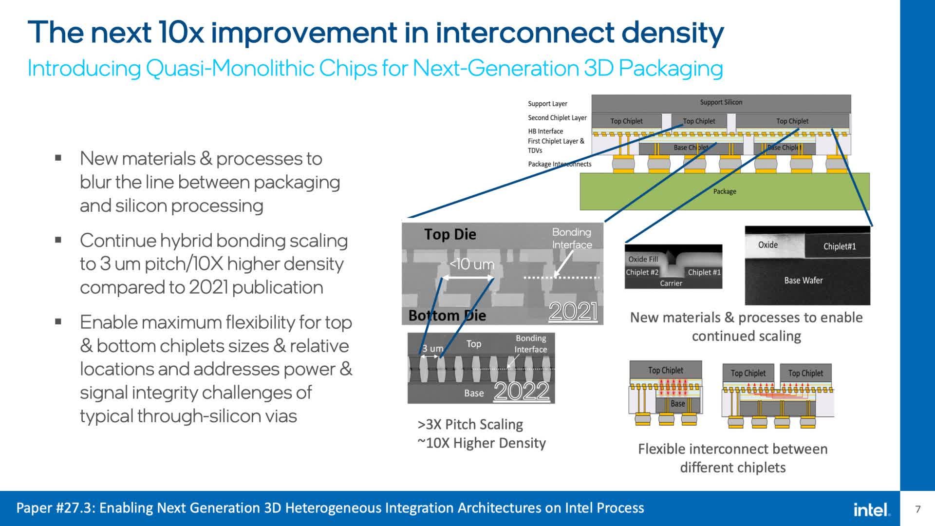
Intel's new transistor and packaging research is primarily focused on advancing CPU performance and efficiency, closing the distance between traditional single-die processors and new chiplet-based designs. Some of the concepts presented in the submitted materials include greatly reducing gaps between chiplets to improve performance, transistors capable of retaining their state even after losing power, and new stackable memory solutions.

Gary Patton, Intel's vice president and general manager of Components Research (CR) and Design Enablement, said that "seventy-five years since the invention of the transistor, innovation driving Moore's Law continues to address the world's exponentially increasing demand for computing. At IEDM 2022, Intel is showcasing both the forward-thinking and concrete research advancements needed to break through current and future barriers, deliver to this insatiable demand, and keep Moore's Law alive and well for years to come."

The CR group's research has identified new processes and materials critical to driving the company closer to their trillion-transistor milestone. The company's latest hybrid bonding research shows a 10x improvement over the previous year's presentation. Other research showcased by Intel's submissions includes designs using novel materials with thicknesses not exceeding three atoms, memory that can be placed vertically above transistors, and a greater understanding of interface defects that can negatively impact quantum data storage and retrieval.

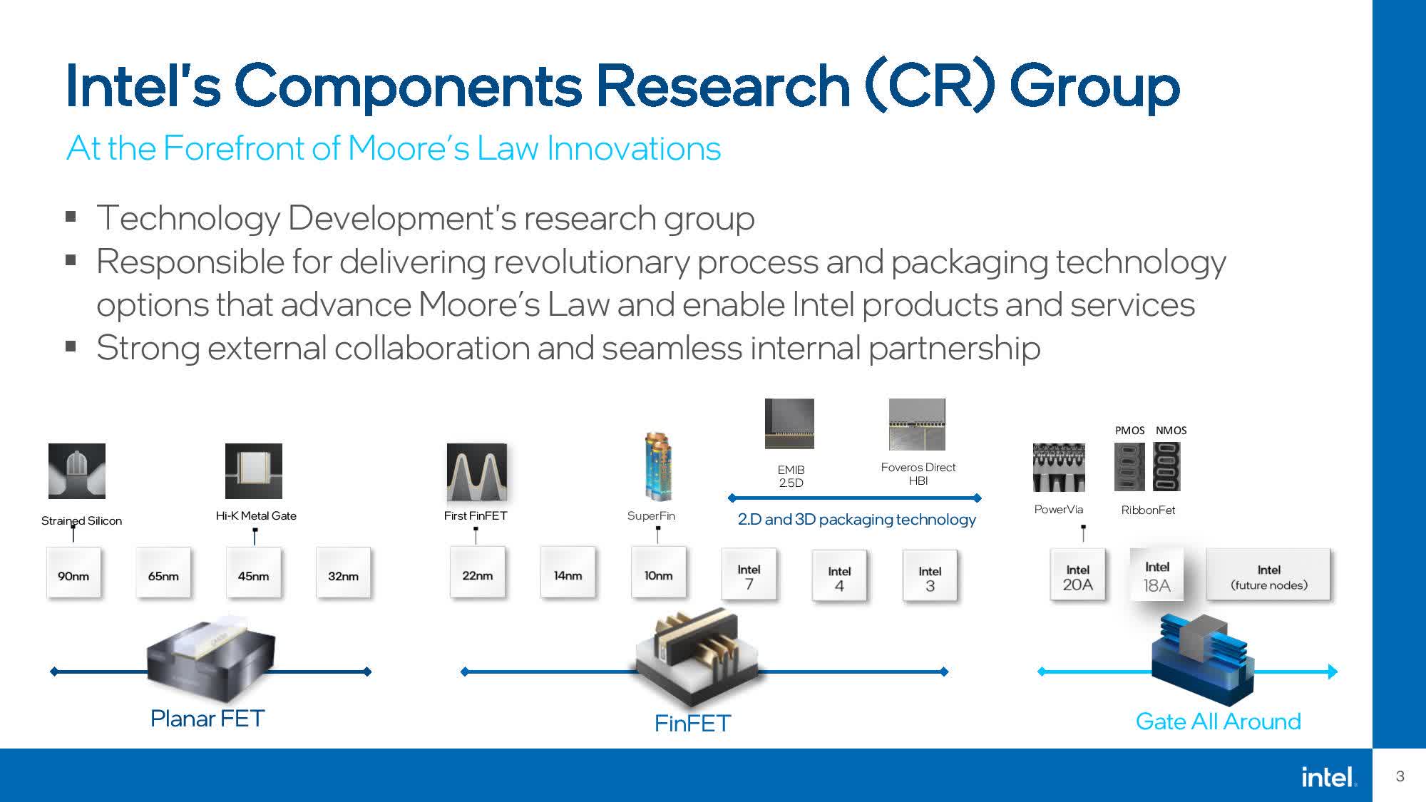
Intel's Components Research Group serves as the company's internal leader for new and groundbreaking technology development. CR engineers invent and develop new materials and methods that support semiconductor manufacturers in the ongoing battle to shrink technology to the atomic scale. The group is responsible for Intel's extreme ultraviolet lithography (EUV) technology, which has been integral to its ability to continue shrinking node sizes while increasing overall semiconductor capabilities. The group's work and timelines are typically five to 10 years ahead of commercially available technologies.

Permalink to story.

 
1.2 Trillion transistors and only 3700 Watts in ECO mode?

When are these laptops available again?

Due to supply chain issues and inflation, Microsoft's $100 Laptop will be on sale around 2037 for the amazing low price of only $12,500 (Plus Tax and shipping)
Pre-Order TODAY!
 
Last edited:
Trillion-transistor chip eh? Are these the same clowns who predicted circa 2008 that the Pentium 4 chips would reach 10Ghz in a few years? How did that work out for them?
Well, given that their Ponte Vecchio GPU has in excess of 100 billion transistors, it’s not beyond the realms of imagination that they could have something with 10 times the count in, say, 10 years. In 2012, the largest monolithic GPU had 7 billion transistors; the largest now is ten times that figure and still monolithic. Once the industry fully embraces tiling and chiplet methodologies, the limitations of monolithic fabrication no longer applies.
 
Trillion-transistor chip eh? Are these the same clowns who predicted circa 2008 that the Pentium 4 chips would reach 10Ghz in a few years? How did that work out for them?
That was like 1998, not 2008.

And yeah, 10 GHz is easily achievable today if we just forget about ipc.
 
Trillion-transistor chip eh? Are these the same clowns who predicted circa 2008 that the Pentium 4 chips would reach 10Ghz in a few years? How did that work out for them?

Most predictions turn out to be wishful thinking. These people seems to forget something called reality.
 
Will it enable CPUs with higher processor frequencies rather than just more cores ?
Probably just more cores. If AMD or Intel wanted higher clock speeds instead high ipc, 10 GHz would not be hard to achieve so that's not big problem.
 
It is very easy to say on paper, but very difficult to execute. Case in point, Intel themselves where they missed their 10nm roadmap by a significant number of years. And to get it into the market, I am pretty sure they had to make some compromises. And their 7nm is also off schedule if I am not mistaken.
 
It is very easy to say on paper, but very difficult to execute. Case in point, Intel themselves where they missed their 10nm roadmap by a significant number of years. And to get it into the market, I am pretty sure they had to make some compromises. And their 7nm is also off schedule if I am not mistaken.
Correct. 7nm will be late at least couple of years. If it finally arrives we can say how much. Intel is doing pretty good so far despite constant delays. Gelsinger can keep looking AMD's backlights.
 
If this is anything like their "legendary road map" from 15 years ago with respect to process width, it's pure bullsh!t for the stockholders. The gullible ones at that.
 
Correct. 7nm will be late at least couple of years. If it finally arrives we can say how much. Intel is doing pretty good so far despite constant delays. Gelsinger can keep looking AMD's backlights.
Meteor Lake uses Intel 4 node which is their version of "7nm". This is from their tech slides:

The 14th Gen Meteor Lake family will leverage four distinct process nodes from different foundries. These include Intel’s 22nm node for the Foveros base tile, Intel 4 for the CPU tile, TSMC’s 5nm node for the iGPU (tGPU), and the N6 process for the I/O and SoC tiles.
Yeah, I won't bother to even remember renamed process names. Intel should stick with originals and make new naming for new ones.
 
If they can hit 1,000,000,000,000 transistors in a chip, this would be proof that Huang was lying when he said "Moore's Law is Dead".

If Moore's Law really were dead, we'd never reach a trillion transistors on a silicon chip because the die would be insanely huge. Using Navi 31 as an example, we have 58,000,000,000 transistors on a die that is 306mm². Doing the math, at our current process node, the size of a die with 1,000,000,000,000 transistors would be about 5,276mm². That's almost 5.3m² of silicon! Can you imagine what it would take to cool the thing?!

Moore's Law must still be in effect because without it, we'll never get to a process node that would allow a transistor count of 1,000,000,000,000 on a single chip.
 
Back