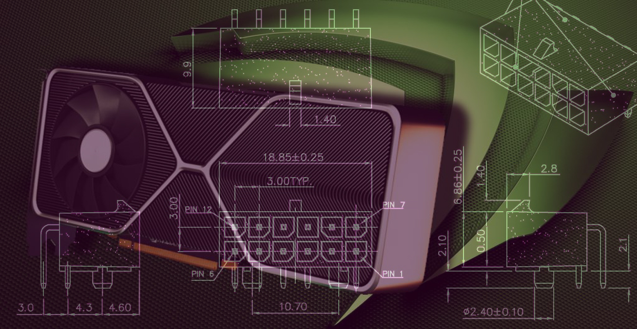
Footprint on the PCB - if you look at the first video image I posted, you can see that the connector sits on the 'V' at the end of the PCB. It doesn't look there would be room for two 8 pin connectors.
what did they do to decrease the footprint? They're still 12V so it needs to provide the same amount of amps. To make the math easy, If you need a total area on the wire of 10mm^2 to provide 30 amps(360w@12v), splitting it up over 12 wires instead of 8 wires isn't going to decrease the overall volume of wire required. Aside from a single image and a claim of "making it smaller while also carrying more power", they didn't really explain anything about it. That said, I did skip through it quickly trying to find anything about them talking about the connector. I actually probably spent more time skipping around than I would have if I just watched it the whole way through.
This is also coming from the company that just went on about thermodynamics
" As Nvidia thermal architect David Haley recounts, the
first law of thermodynamics states that energy cannot be created or destroyed in a closed system. "
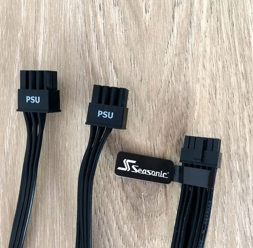
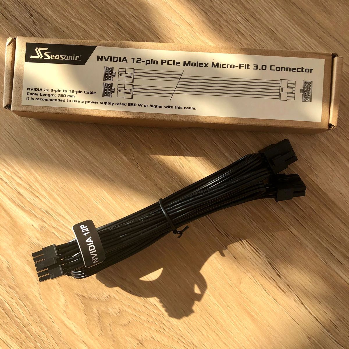
Ddoes physics only apply when nVidia wants it to? Also, I looked up the adapter online, it uses 2X8pin to 12pin adapter, at least that's what Anandtech said. They designed and patented their 12 pin connector, they're likely to charge PSU manufactures to put it on because "mUh NvIdIa". There will start being "Geforce Ready" or "RTX ready" powersupplies that's nothing but marketing that they can charge other companies for. "give us money and you can put a sticker on your product"
nVidia makes this stupid card with a stupid cooler and then they have to design an entire power connector around it to fit. The fact that the card is the largest PCIe card I've ever seen and they have to make a whole new power connector just to make it fit, or whatever, really makes me question the hype of the 3000 series. It's bigger in every dimension than the last cards, height, width and depth, atleast that's what I get from the pictures. They need to make a special connector because 2 8pin wont fit?
Going into the connectors, PCI-E power connector math really doesn't make any sense. 6 pin provides 75watts and 8pin provides 150w? I don't understand how adding another negative and positive wire adds 75 watts if a 6 pin is 3 negative and 3 positive. If we want to do some math, each wire can only carry 25watts(or ~2A@12V). I don't understand how going to 8 pins magically makes the same gauge wire capable of ~3amps. I will say that I've salvaged wire from PSU's to use them in other things and pushed them well past the 20amp@12v mark on a single wire.
This whole thing is the GPU equivalent of taking the headphone jack off the iPhone to make it thinner, but instead they made it just gets bigger anyway.

")