Samsung puts fifth-generation V-NAND memory into mass production

Greg S

Posts: 1,607   +442
Something to look forward to: Even faster solid state drives are on the horizon as Samsung begins mass production of its next generation V-NAND memory. Improvements in manufacturing offer better performance and higher yields of usable chips.

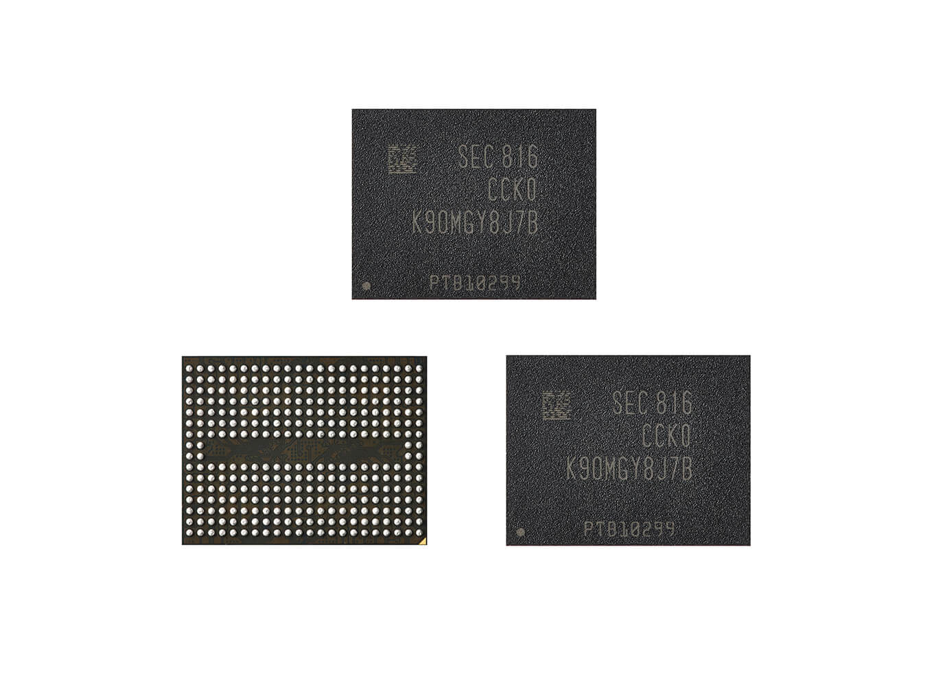
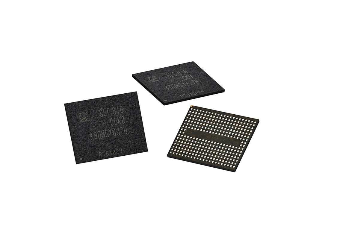
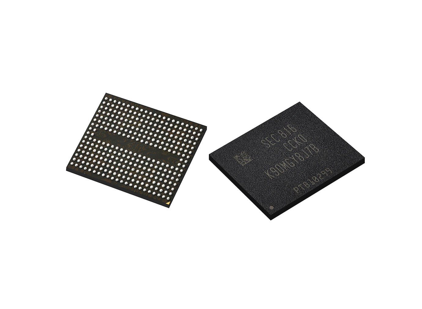
Samsung has begun mass production of its fifth generation V-NAND memory. Using over 90 layers compared to the previous generation's 64, the new memory achieves nearly a 40 percent improvement in performance.

Fifth generation chips arrive in 256 gigabit (32GB) capacities. Each chip can reach speeds of up to 1.4 Gbps and makes use of the Toggle DDR 4.0 interface. Despite having more layers, the chips are not all that much thicker. A 20 percent reduction in layer thickness has been achieved as a result of improvements made to the atomic layer deposition process used during fabrication.

Energy efficiency remains roughly the same since Samsung is able to run its newest generation at 1.2 volts instead of 1.8 volts. Write speeds have been improved by up to 30 percent. Samsung also boasts that its V-NAND can achieve the highest peak write speeds on the market with bits of data being stored in as little as 500 microseconds.

Roughly 85 billion charge trap flash cells can be found inside the fifth generation chips each storing three bits of data. All cells are contained in a pyramid structure with vertical channels that are a few hundred nanometers wide.

Even though manufacturing processes have become extremely expensive for semiconductor components, Samsung reassures us that productivity is up over 30 percent. Faster storage may not be any more expensive than current generation products.

Later this year, Samsung is planning to introduce 1-terabit V-NAND chips and will also be adding quad-level cell products to offer even higher capacity options.

Permalink to story.

 
I'm confused, why does the increase in layer density amount to "nearly a 40%" increase in performance?

I'd presume "capacity", not performance, yes?
 
I'm confused, why does the increase in layer density amount to "nearly a 40%" increase in performance?

I'd presume "capacity", not performance, yes?

This article doesn't specifically mention what causes the increased speed. That said, everytime you shrink the size of a component you make it faster as the electricity has a smaller distance to travel.
 
I'm confused, why does the increase in layer density amount to "nearly a 40%" increase in performance?

I'd presume "capacity", not performance, yes?
Yep presume a typo as those figures don't seem to directly correlate. The article later cites write perf is up only 30% which implies to me that read performance improved less than 30% so I deduce that both read and write perf improved less than 40%.
 
That said, everytime you shrink the size of a component you make it faster as the electricity has a smaller distance to travel.

Ehh, that's a bit of an oversimplification. On NAND flash, both reads and writes tend to get slower as you shrink the lithography. The best link I was able to quickly find was one from Anandtech's Crucial M500 review (see table in the middle of the first page), but I'm pretty sure they did a followup piece that included more types of NAND -- I just can't find that article. Combating this effect was one of the advantages of moving to 3D NAND. At least initially it wasn't the 3D-ness of the flash that was making it faster, it was the transition back up from 15/16nm to ~40nm. I'm intentionally leaving endurance out of the discussion since it it not the topic at hand.

That said, here they aren't shrinking the lithography - just the distance between layers. I could see shorter traces reducing latency.

Assuming that the nearly "40 percent improvement" isn't a typo or bad choice of words, it could also be that the sentence is mistakenly implying causality that does not exist. In other words, the new V-NAND might offer ~40% more performance, but that increase might not be due to the additional layers. I haven't been able to find what the specs of the Toggle DDR 3.0 interface are (presumably what the previous generation of V-NAND is using) but it might be something as simple as each NAND die now has a 1.4Gb/s interface instead of a 1.0Gb/s interface.

Not saying whether either NAND die can saturate its link, but I could see how a press release might be ambiguously worded to make it seem like the interface speed increasing by 40% was a 40% improvement in overall improvement.

I think the title of that table is appropriate

"Intel/Micron NAND Evolution"

It doesn't make any claims to any NAND trend in general of products getting slower as they shrink. If they did they would definitely have to explain that phenomenon as it's contrary to physics.

Unfortunately we have no idea where that performance increase is coming from so all we can do is guess. Benchmarks will tell us for sure if their performance claims are real when drives come out using these.
 
Back