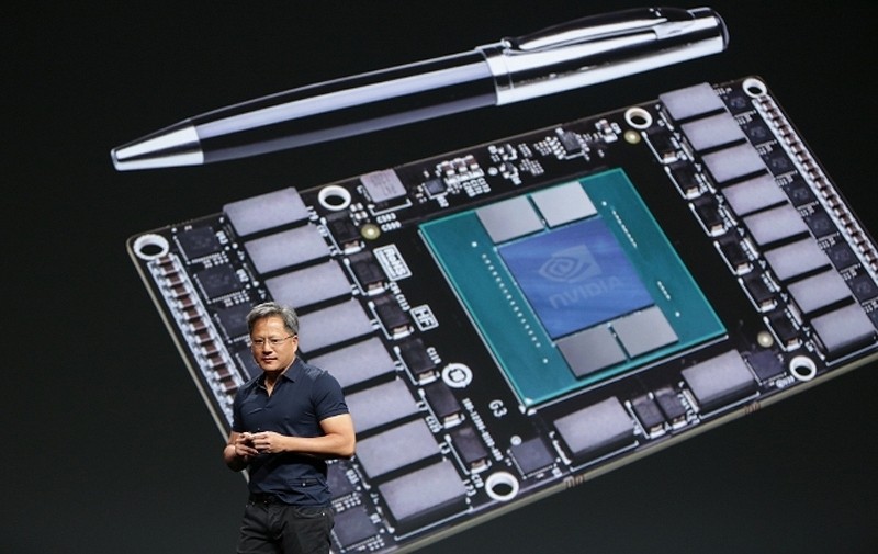
Nvidia chief Jen-Hsun Huang revealed the successor to Maxwell during the company's annual GPU Technology Conference in San Jose, California. Named after 17th century French mathematician Blaise Pascal, the Pascal GPU is more than just an incremental update as it will circumvent the PCI Express bus to provide more bandwidth between the CPU and GPU.
Pascal won't ship anytime soon but there's plenty to get excited about in the meantime. Instead of the tried and true PCIe interface, the GPU will utilize a new socket called NVLink that was co-developed with IBM. It'll offer speeds up to 12 times faster than what is currently possible over PCIe.
Cards that utilize this new interface will be smaller and much more energy efficient thanks largely in part to the use of a technique called stacked DRAM, or 3D memory. As the name suggests, this configuration allows chips to be stacked on top of each other and will help push memory bandwidth to 1000 times where it is today.
Elsewhere, unified memory will allow applications to take advantage of both the CPU and the GPU. Specifically, the CPU will be able to access the GPU's memory and vice-versa. This means that developers will no longer need to allocate resources between the two processors.
Nvidia's claim of Pascal's package being smaller was no joke as the reference board Huang showed during the keynote was about a third of the size of a typical PCIe video card.
The new platform will arrive sometime in 2016 geared toward gaming, cloud computing, supercomputing and machine learning.
