A brief explanation why
For years, "integrated graphics" technically lived near the CPU – but not on it. Early PC platforms paired a CPU with a northbridge chipset containing a GPU, and later, some products placed a GPU on the same package but still not on the same die. This distinction is subtle but important: on-package ≠ on-die.
A popular wrong guess is Intel Clarkdale / Arrandale (2010). These were the first consumer Core i3 and Core i5 parts with "Intel HD Graphics" branding: popular SKUs included the Core i5-661, i5-650, i3-540, and the mobile i5-430M. However, those CPUs actually used a multi-chip module (MCM): one die housed the CPU cores on 32 nm, and a second separate 45 nm die contained the GPU and memory controller. They shared a substrate, not silicon. Marketing blurred the lines, but architecturally, the GPU still wasn't part of the CPU silicon.
Another tempting answer is AMD Llano (2011), and this one is very close. Llano truly brought a GPU onto the same die as the x86 cores and introduced the "APU" branding that AMD still uses today. Llano used K10-based CPU cores and a Radeon-class GPU on a single piece of silicon. Consumer models included the AMD A8-3850, A8-3500M, and A6-3650. However, Llano shipped months after Intel had already crossed the finish line.
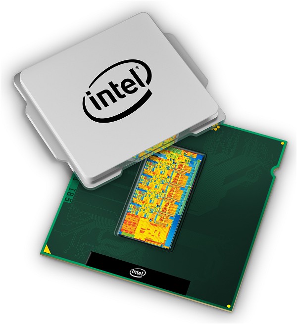
The correct answer to our trivia is Intel Sandy Bridge, launched January 2011. Sandy Bridge was the first consumer CPU to place a GPU and CPU cores on a single, monolithic die, sharing caches and a common ring bus fabric. This marked the actual birth of fully on-die graphics in the consumer space. Well-known models include the Core i5-2500K, i7-2600K, i5-2400, and the mobile i7-2720QM. The GPU was no longer a bolt-on component – it became a first-class citizen of the CPU's execution complex.
Sandy Bridge was widely regarded as a breakthrough generation, one of Intel's biggest architectural wins of the 2010s. Reviewers praised its performance-per-watt, huge IPC gains over Nehalem/Westmere, strong Turbo Boost behavior, and shockingly fast hardware video encoding via Quick Sync.
Even enthusiasts who never used the iGPU recognized that the die-level integration enabled tighter power gating and thermal budgets, contributing indirectly to CPU performance. Sandy Bridge was also a massive commercial success; the i5-2500K, in particular, became a legend among gamers and remained viable for many years.
This shift had long-term architectural consequences. Power management improved dramatically because the graphics and CPU domains could cooperatively share thermal and electrical budgets. Memory latency dropped, frame pacing improved, and media encode blocks became tightly integrated with CPU-side scheduling. Sandy Bridge set the template for what we now simply call a "modern CPU": heterogeneous compute resources stitched together on the same slab of silicon.
So while multiple earlier platforms shipped with "integrated graphics," Sandy Bridge is the first CPU to host graphics on the same slab of silicon – the true dawn of the modern "CPU + GPU on one die" era.