25 Years Later: A Brief Analysis of GPU Processing Efficiency

Julio Franco

Posts: 9,097   +2,048
Staff member
Just get a AMD gpu drop power down 15% and save 100+ watts. Overclock memory 10% and take back what you lost.
 
Last edited:
Just get a AMD gpu drop power down 15% and save 100+ watts. Overclock memory 10% and take back what you lost. You be on point with Nvidia on efficiency then. What I do.
To avoid accusations of bias or fanboyism, it's generally more honest to stick with like-for-like comparisons (stock vs stock or undervolt vs undervolt) given that you can do exactly the same aggressive undervolting on nVidias too (link). It's certainly possible to take a 208w RX 580 and undervolt it to compare it to a stock 120w GTX 1060. But it's also equally possible to undervolt a 100w GTX 1650 SUPER down to 75-80w then compare that to a stock 208w RX 580 (link)...

If people are going to do GPU efficiency comparisons, then they need to be honest, consistent and actually compare them using the same methodology.
 
Here, I share a video I watched couple of days ago. This gives a clue (or perspective) how and why Nvidia architecture may be more efficient, according to coretex
 
To avoid accusations of bias or fanboyism, it's generally more honest to stick with like-for-like comparisons (stock vs stock or undervolt vs undervolt) given that you can do exactly the same aggressive undervolting on nVidias too (link). It's certainly possible to take a 208w RX 580 and undervolt it to compare it to a stock 120w GTX 1060. But it's also equally possible to undervolt a 100w GTX 1650 SUPER down to 75-80w then compare that to a stock 208w RX 580 (link)...

If people are going to do GPU efficiency comparisons, then they need to be honest, consistent and actually compare them using the same methodology.
No you wont get same returns on Nvidia because they are clocked lower down on the power graph.
AMD is on a steep slope Nvidia isnt.
AMD struggle to keep up so they push the envelope and that is why they save so much power when you lower the power target.
 
Last edited:
No you wont get same returns on Nvidia because they are clocked lower down on the power graph. AMD is on a steep slope Nvidia isnt.
Exact returns are less important than the endless apples & oranges comparisons. This comment isn't aimed at you personally, but if people started comparing the latest power hog Intel's only by undervolting them vs stock Ryzen's to try and hide +50-100w excess power consumptions, then declared them "on point" with Ryzen's efficiency on the back of highly skewed stock vs undervolt disparities, people would rightfully be calling out fanboyism / bias. It's just as true the other way around with the dishonest habit of measuring AMD's space heater GPU's differently until they show the "correct" result. The only honest people who both want to undervolt but also simultaneously want to then compare the resulting power efficiency across brands are those who undervolt for all brands if they do it for one. Period.
 
Last edited:
Yeah Ryzen TDP is a load of bs.
Says its a 65 watt cpu but in reality it pulls far more.
This 3700x I have pulls 125 watt at stock clocks.
my rest power usage is 100 watt at the wall but under full load in AIDA64 it hits 225 watt.
Thee is a option in bios to set it to 45 watt but the clock speeds are a joke if you set that option but its very efficient .
 
All these stated TDP and watt range are all subject to user manipulation.
CPU and GPU can be changed to users preference.
My Vega card is one hungry card If I slide the power target to +50% but I dont gain any performance in games but in compute tasks I do. Its one strange card. I've given up trying to fight it out. I set it to power save mode now and clock hbm2 to 1150 mhz and just use the thing.So long as its silent and cool who cares.
 
All I care about is having 10 bit 1 billion colours vs nvidia 16 million and mixed mode eyefinity that works in full screen. Try this on nvidia you will get a stretched image because only way for them is window mode.
 
No you wont get same returns on Nvidia because they are clocked lower down on the power graph.
AMD is on a steep slope Nvidia isnt.
AMD struggle to keep up so they push the envelope and that is why they save so much power when you lower the power target.

Based on the 4 Nvidia GPUs I've undervolted and overclocked (1050Ti, 1060-6, 1080, 1660S), I have to agree with this assessment. All cards are manufacturer OC but really can take higher OCs at full and over- voltage, even the 1050Ti which is a slot-power only model. However the power savings is only ~25% if you undervolt (usually to ~0.85-0.88v) while maintaining the card's shipping MHz and put a max OC on the memory.

Sure, you can UV some more and lower performance and power draw but I only do that for older or lower-spec games. For instance Rocket League uses ~65W @0.7v and 1480 MHz on the 1080 at 1440p/144Hz.

Using Afterburner, you can look at the voltage curve yourself and see that above 0.9v that curve flattens out pretty quickly, you're nopt getting much more performance for the increased voltage and power. Nvidia GPUs out of the box run at 1.01v to 1.05v depending on the quality of cooling so they're not too far off the 0.9V setting that I'd describe as optimal for performance and power. I really want an RX 570 to see how this works on the AMD side.
 
Hmm...the author kinda forgot TU102 has dedicated die space for Raytracing and tensor cores and GV100 has tensor cores also.
If we compare Vega 10 and GP102, they are not so far apart in GFLOPs per die space but GP102 is leagues ahead in GFLOPs per TDP, and that is we don't take in account the HBM die space...
 
Not so much forgotten, but more a case of you have to ignore something for a simple analysis like this. For example, a fully unlocked Vega 20 (as used in the Raden Instinct M160) has pretty much the same FP16, FP32, and FP64 throughput as a GV100, but the latter obviously has the tensor cores which can be used in parallel with the shader units. However, they do an FP16 multiplication, followed by an FP32 addition, so it's not a case of just adding the numbers all together.

With regards to the tensor and RT cores, it's worth nothing that a TU116 is 284 mm2 and the TU106 is 445 mm2 in area; the former has 24 SMs to the latter's 36, so if one scales the TU116 by a factor of 36/24 then its area becomes 426 mm2. Of course, the TU116 has no RT core or the 4 sets of Tensor cores per SM that the TU106 has, but they've been replaced by 4 sets of 32 FP16 ALUs. The TU116 also has 2 fewer memory controllers, but the rest of the architectural layout (TPC and GPC count) is the same in the two chips, so the the extra 19 mm2 of die space accounts for the 2 memory controllers and the size difference between the tensor+RT cores versus the banks of FP16 ALUs.

So how big are the tensor and RT cores? Well, if you take a die shot of the TU102, you can hack out a rough estimate:

813-die-shot.jpg


This is 754 mm2 of die area, and architecturally has the following layout:

813-block-diagram.jpg


813-sm-diagram.jpg


Now assuming the 2nd and 3rd images are accurate layout representations of the die shot, SM units are roughly 12 mm2 each and RT cores account for 0.6 mm2 of that or 5%. Working out which sector in the die image are the tensor cores is harder, but a total guess puts it around the same as the RT block.

So in total, the tensor and RT cores account for (very, very, very approximately) 12% of the whole die. If such guessing is fairly close to the mark, then removing these units from the analysis would shift the position of the Turing and Volta chips, but not by that much.

You do make a good point about the inclusion of the HBM affecting the die size figures (I.e. AMD's Fiji and Vega, Nvidia's GV100), so I'll have a look at some die images and estimate the actual GPU sizes - I'll post updated graphics in this thread to see what change this has.

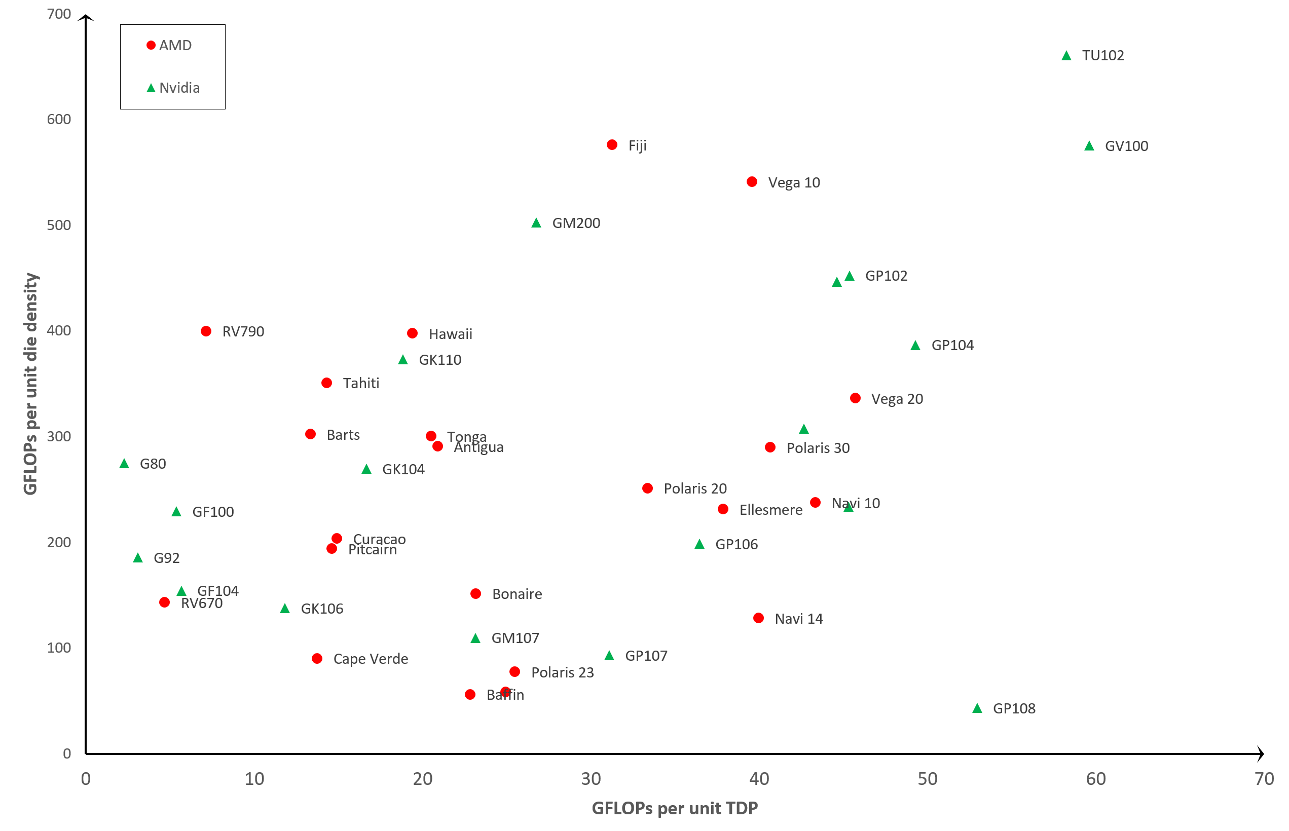
Edit: Here are the adjusted graphs for the removal of HBM with die area. TDP values remain the same, as they are for the whole card, but it's not been possible to adjust the transistor count as it's not clear whether AMD or Nvidia include the HBM's transistors in the total count.

tdpvsdiedensity_noHBM.png
tdpvsdiearea_noHBM.png

The Vega 20 chip is missing off the 2nd graph because it's GLOPs per unit die area comes to a value of 101, so it's way above the rest. The actual Vega 20 chip is pretty small:

848-vega-20-xt.jpg


The HBM itself actually has more die area than the GPU.
 
Last edited:
Lol, Navi 10, a 7nm GPU is worse in efficiency than Pascal a 2016 16nm GPU. That is what I call s**t efficiency.
 
Yeah Ryzen TDP is a load of bs.
Says its a 65 watt cpu but in reality it pulls far more.
This 3700x I have pulls 125 watt at stock clocks.
my rest power usage is 100 watt at the wall but under full load in AIDA64 it hits 225 watt.
Thee is a option in bios to set it to 45 watt but the clock speeds are a joke if you set that option but its very efficient .
Hey heard of the Intel 65 watt 10th gen cpu consuming over 230 watts hahahahahaha by that standard Intel TDP is utter load of horse **** mixed with raw sewage
 
You mean Intel TDPs are full of shat. The TDP you are talking about is boost clocks and not default operating power.
 
Back