AMD patent proposes new memory module to double DDR5 speeds

Skye Jacobs

Posts: 1,917   +58
Staff
The takeaway: AMD is exploring a new approach to system memory that could reshape the trajectory of DDR5, which has struggled to keep pace with the performance demands of gaming, artificial intelligence, and data-intensive computing. A recently published patent, first reported by Tech4Gamers, outlines what the company calls a "high-bandwidth memory module architecture" – a design intended to extend the usefulness of DDR5 technology without requiring fundamental changes to its underlying chips.

The patent describes the development of high-bandwidth dual inline memory modules (HB-DIMMs) that use pseudo channels and specialized data routing to boost performance. Rather than re-engineering DRAM chips, AMD proposes coupling multiple DRAM devices to advanced data buffer chips. These buffers manage signal flow in a way that effectively doubles output, raising transfer speeds from the current 6.4 gigabits per second to 12.8 gigabits per second on the memory bus.

By working within the framework of established DRAM architectures, the design positions itself as an upgrade that could be adopted without industry-wide overhauls to manufacturing or platform standards. AMD argues that DDR5 in its current form is hitting performance ceilings just as system workloads are rapidly expanding.
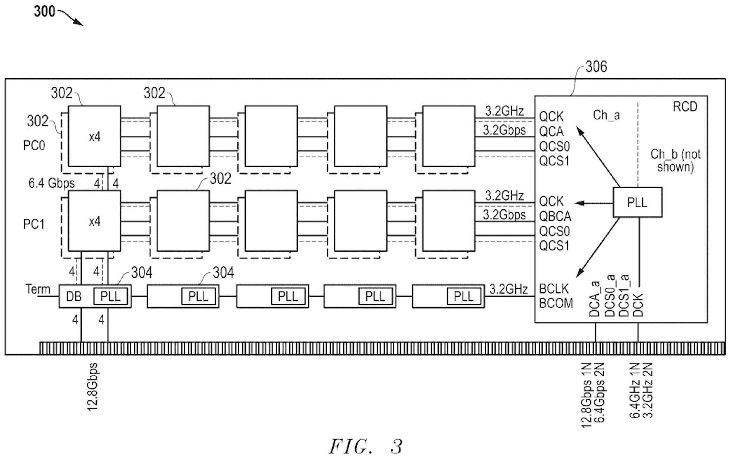
At the core of the architecture is a register clock driver circuit that decodes memory commands and routes them using a chip identifier bit. This approach allows the module to assign tasks to independently addressable pseudo channels, enabling true parallel access rather than the sequential limitations that typically constrain throughput.

The system also supports both 1n and 2n operating modes, providing flexibility in how clocks and signals are managed. This adaptability helps optimize timing margins, ensures compliance with DDR5 requirements, and reduces signaling complexity. Rather than relying on interleaved configurations, AMD's proposal adopts a simplified non-interleaved transfer format that lowers latency and improves signal integrity.
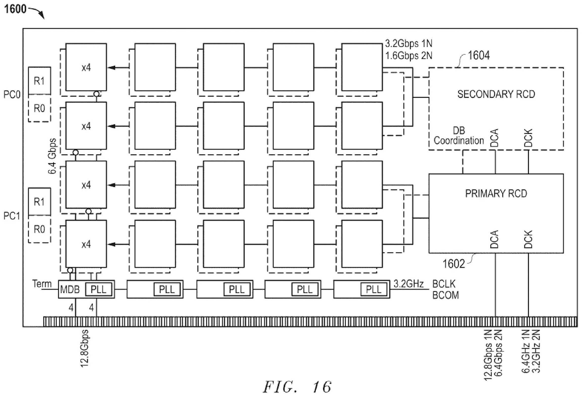
Another feature of the design is its ability to switch between pseudo-channel operation and quad-rank configurations. This versatility makes it well-suited for high-performance computing scenarios, where striking a balance between throughput and flexibility is often critical. The broader goal is to reduce reliance on entirely new chip designs for memory scaling, instead focusing on extending the capabilities of existing DRAM technologies.

Tech4Gamers notes that this isn't the first time AMD has sought to address performance bottlenecks through incremental but impactful engineering advances. Recent patent filings include a blower fan design aimed at improving thermal management in gaming laptops and a cache-memory cleaning system intended to boost processor efficiency.

Permalink to story:

 
If this pans out, future iGPUs could get a massive boost. Although I wonder if this technique could also be applied to dGPU VRAM too?
 
If this pans out, future iGPUs could get a massive boost. Although I wonder if this technique could also be applied to dGPU VRAM too?

The real question might be whether discrete GPUs will remain necessary, or if supercharged APUs will dominate 90% of the market. For AMD, integrating CPU and GPU into a single package is strategically advantageous, as it avoids profit-sharing with AIB partners. Plus, using this IP with LPDDR6 could already surpass the bandwidth offered by GDDR6.
 
Don't forget that AMD co-developed HBM with SK Hynix, and look where HBM is now (though it took a while).

This HB-DIMM is interesting, as long as latency is controlled and predictable (for CPU side), this can certainly be a boon to iGPUs, which are not sensitive to RAM latency and need throughputs for their parallel workloads.

Going this route is likely more power efficient than trying to get SoC/IOD Infinity Fabric to scale to ever higher RAM speeds or doubling memory bus widths to 256-bit on mainstream platforms.
 
The real question might be whether discrete GPUs will remain necessary, or if supercharged APUs will dominate 90% of the market. For AMD, integrating CPU and GPU into a single package is strategically advantageous, as it avoids profit-sharing with AIB partners. Plus, using this IP with LPDDR6 could already surpass the bandwidth offered by GDDR6.
The size still matters. You can pack so much more power into the space GPU takes compared to APUs. And with engines as unoptimized as U5 for example, we will need that extra power.
 
The size still matters. You can pack so much more power into the space GPU takes compared to APUs. And with engines as unoptimized as U5 for example, we will need that extra power.
It doesn't change the strategy here. The cost of large dies will be so high that I doubt it will matter to most mid- or low-end buyers, and AMD can make very large modular APUs.
 
Fun fact, chipsandcheese did a detailed analysis of the 9950X performance and found it literally needs DDR5 20000 to feed the cores properly, that's how much bandwidth it requires and yet AMD is stuck on 8000 at best. Maybe they need to offer quad channel memory. Infinity fabric is way out of date and hopefully the rumours of a much faster interconnect fabric for Zen 6 are true supporting much better DDR5 rates at least 8533 at 1:1.
 
It doesn't change the strategy here. The cost of large dies will be so high that I doubt it will matter to most mid- or low-end buyers, and AMD can make very large modular APUs.
The era of large dies is coming to an end, soon all chips will consist of multiple smaller dies.
 
They already “inflate” out usual folks from big fat gpus with schizo prices, look at second tier 5080 going for 2K usd.
Not long until nvidia-amd-alike just abandon big-chip-for-games design, leaving only 100mm2 chicken **** dies for you and motivating it like “we sent all the bulk silicon on AI, you get whats left, you dont need more, we said so”.

Why not put it under APU altogether then?

P.S. imagine APU with granite ridge x3d die and navi 48 in one package

Why buy a used 5080 for $2k when I can get a new 9070 XT for under $700?
 
Why buy a used 5080 for $2k when I can get a new 9070 XT for under $700?
I've meant second tier after 5090, not used card, though that's also fair point, few ppl already trying to sell their half year old 5080s asking like it's brand new.

But anyway, to be fair if we compare 2K 5080 then we should take 1K$ variant of 9070XT. There are low quality 5080s available for ~1300$ vs 9070XT for ~750$.

I'm not even talking about 15% faster raster performance or ~2x PT performance premium for 5080
 
Back