CPU and GPU SRAM caches are not shrinking, which could increase chip cost or reduce performance

AaronK

Posts: 13   +0
Why it matters: An interesting article posted at WikiChip discusses the severity of SRAM shrinkage problems in the semiconductor industry. Manufacturer TSMC is reporting that its SRAM transistor scaling has completely flatlined to the point where SRAM caches are staying the same size on multiple nodes, despite logic transistor densities continuing to shrink. This is not ideal, and it will force processor SRAM caches to take up more space on a microchip die. This in turn could increase manufacturing costs of the chips and prevent certain microchip architectures from becoming as small as they could potentially be.

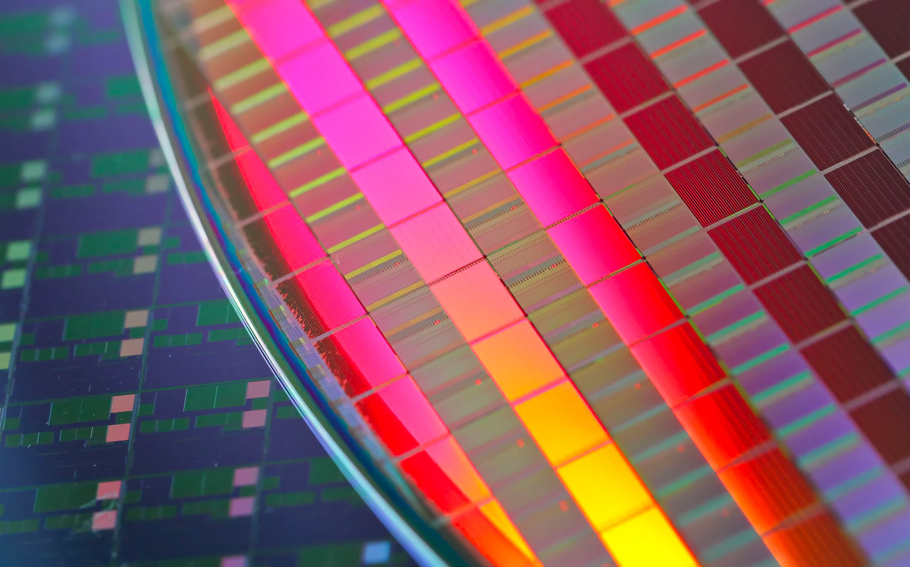
Nearly all processors rely on some form of SRAM caching. Caches act as a high speed storage solution with very fast access times due to their strategic placement right next to the processing cores. Having fast and accessible storage can significantly increase processing performance and result in less wasted time for the cores to do their work.

At the 68th Annual IEEE International EDM conference, TSMC revealed huge problems with SRAM scaling. The company's next node it is developing for 2023, N3B, will include the same SRAM transistor density as its predecessor N5, which is used in CPUs like AMD's Ryzen 7000 series.

Another node currently in development for 2024, N3E is not that much better, featuring a measly 5% reduction in SRAM transistor size...

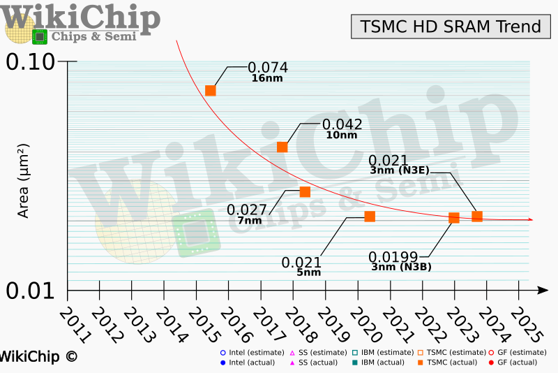
For a broader perspective, WikiChip shared a graph of TSMC's SRAM scaling history from 2011 to 2025. The first half of the graph -- representing TSMC's 16nm and 7nm days -- shows how SRAM scaling was not a issue and how it was getting smaller at a rapid pace. But once the graph hits 2020, scaling basically flatlines, with three generations of TSMC logic nodes using nearly identical SRAM sizes: N5, N3B and N3E.

With logic transistor density still increasing at a rapid pace -- up to 1.7x in the case of N3E -- but without SRAM transistor density following the same path, SRAM will start consuming a lot of die space as time goes on. Wikichip demonstrated this with a hypothetical 10 billion transistor chip, operating on several nodes. On N16 (16nm), the die is large with just 17.6% of the die area composed of SRAM transistors, on N5, this goes up to 22.5%, and 28.6% on N3.

WikiChip also reports that TSMC isn't the only manufacturer with similar problems. Intel has also seen noticeable slowdowns in SRAM transistor shrinkage on its Intel 4 process.

Unless this is somehow remedied, we could soon see SRAM caches consuming as much as 40% of a processor's die space. This would lead to chip architectures having to be reworked and add to development costs. Another way manufacturers might cope is to lower cache capacity altogether, which would reduce performance. However, there are alternative memory replacements being looked at, including MRAM, FeRAM, and NRAM, to name a few. But for now, it remains a challenge with no clear answer in the immediate future.

Permalink to story.

 
I thought the answer would be 3D cache. Using the cache on older, cheaper processes while the rest of the CPU benefits from the newer node.
 
I thought the answer would be 3D cache. Using the cache on older, cheaper processes while the rest of the CPU benefits from the newer node.
I believe 3D V-cache is L3 cache, which is even slower than L2, which in turn is slower than SRAM. L2 and L3 caches are very different from SRAM, which is much closer to the CPU core and much faster too.
 
Could they put the SRAM on separate chiplet and look at super-high speed interconnects?
I doubt such interconnect exist now. I ve read about travel distances between PC components. Stuff on CPU has such high requirements regarding pathway that there is no way to move it anywhere further.
 
I doubt such interconnect exist now. I ve read about travel distances between PC components. Stuff on CPU has such high requirements regarding pathway that there is no way to move it anywhere further.
As far as I'm aware, AMD's infinity fabric is the only thing remotely close to a commercially produced interconnect. And as amazing as a technology is, it's not nearly fast enough for SRAM. The other thing is that the SRAM is next to logic sectors drasticly reducing latency. Maybe if we had some type of photonic interconnect we could get close but that's probably over a decade away.
 
Well just need that transistor memory duality stuff - or and either or thingy stuff ( that can flick purpose on the fly )
 
I wonder if any stacked interconnect can really make this work. Trace distances on chip at these scales from SRAM to logic have to be measured in hundreds of nm, maybe even a few micrometers at worst. I think all the 3D stacking technologies with micro solder balls are still multiple micrometers at best if not even more. Probably looking at a few orders of magnitude longer trace distances just to package SRAM on a stacked die.

Then, I am sure as you jump across the dies, the power/signal has to be amplified to cross the joint that almost assuredly has much higher resistance/capacitance/impedance than on planar etched silicon, so not only does your trace distance increase but the signal has to get routed though an amplifier. I am not an electomagican though, just guessing.

Latency surely will kill stacking as a viable method.

So, new architectures that are less SRAM reliant as suggested? Surely allocating die area to optimize performance/area is nothing new to chip designers, this just modifies another variable. Makes cooling easier though, I think the SRAM tends to produce less heat per unit area than logic. Also, I think SRAM is still easier to etch without defects, so yield may increase as SRAM area fraction goes up.
 
Last edited:
I believe 3D V-cache is L3 cache, which is even slower than L2, which in turn is slower than SRAM. L2 and L3 caches are very different from SRAM, which is much closer to the CPU core and much faster too.
All cache levels in a CPU and GPU are SRAM, unless explicitly stated otherwise (e.g. some older Intel CPUs had embedded DRAM for the integrated GPU that could be used as a L4 cache by the rest of the processor).

I thought the answer would be 3D cache. Using the cache on older, cheaper processes while the rest of the CPU benefits from the newer node.
Stacking cache dies won't make it any faster -- quite the opposite, in fact. Increasing cache sizes and physically increasing trace lengths only make latencies worse. Traditionally this has been countered in two ways: (1) by reducing the size of the bit cells, by using smaller process nodes, and (2) by increasing clock frequencies. As the news article points out, method (1) is becoming increasing less viable
 
Can anyone briefly explain why the logic circuitry can still be shrunk but the cache circuitry has now reached a limit? Some folk have mentioned that AMD's 3D Cache isn't the answer but the 5800X3D seems to compare well with CPU's a generation ahead. Lastly, how much cache (L1, L2 and L3) do we need, is it always a case of more is better?
 
Can anyone briefly explain why the logic circuitry can still be shrunk but the cache circuitry has now reached a limit?
SRAM is essentially a grid of transistors but it requires a whole host of supporting circuitry to operate reliably at the ever-decreasing voltages used in modern chips. Unlike an FP32 fused-multiply-add unit, which are fairly standardized now, SRAM bitcells are highly specialized in design and fabrication, and what works well in one fabrication node, doesn't automatically translate into another.
Some folk have mentioned that AMD's 3D Cache isn't the answer but the 5800X3D seems to compare well with CPU's a generation ahead.
Games use a lot of repeated data, so having lots of cache in the CPU can help reduce the need to keep hitting the system memory all the time. Zen 3 and later chips route all DRAM operations through the separate I/O die, so it's better to rely on cache as much as possible -- well, this is true for all CPUs, but it's especially the case with those Ryzen processors.
Lastly, how much cache (L1, L2 and L3) do we need, is it always a case of more is better?
In a perfect world, DRAM would be super fast and would take just a few clock cycle to fetch and send the data requested. However, in the real world, DRAM takes 1000s of cycles to do this, hence the use of SRAM (which does the same thing in 10s of cycles) inside the CPU.

The only problem is SRAM is pretty big and takes up a lot of die space, relative to processing logic. Which is why CPUs have multiple cache levels -- starting with very small amounts right next to the logic cores that store instructions and data associated with the threads being worked on at that time. But because this is so small, it can't hold very much for thousands of threads that can pushed through the system.

So you have another amount of SRAM, larger in size but further away, and holds data that's either been pushed out of the first level of cache or that's been prefetched by the CPU. This naturally has limits too, hence why CPUs have a third level, that's even larger but further away still.

Take the Zen 3 architecture, as an example. Each core has 32kB of cache to store instructions and another 32kB for data -- the so-called L1 caches. These amounts have barely changed over the entire Zen history; the first release had more instruction cache but this was shared by two threads. Ever since Zen 2, they've both been 32kB.

Each core also has 512kB of Level 2 cache that holds all of the L1 data, as well as other stuff. The difference between the two levels comes down to the number of cycles it takes to read data from them -- around 6 cycles for L1 and at least 12 for L2.

A cluster of 8 cores share 16 or 32MB of L3 cache (depending on the CPU model). This just stores data that's been booted out of L2, so it can be quickly accessed again if required, but this still takes over 40 cycles to do.

In Zen 4, the L2 cache was doubled in size, so one might wonder why aren't all the caches just doubled like this. The larger the cache, the longer it takes to go through it and read/write the data. Sometimes, through clever design, this increase can be heavily minimized. For Zen 4, the L2 latency is only a handful of cycles longer but the L3 latency is around 10% more.

The amount of cache required very much comes down to the processor's application -- GPUs these days have more cache than a typical CPU, because it has to process a lot more data in parallel. For example, in RDNA 3, each Compute Unit has 32kB to store instructions and 32kB to store general data (AMD label the latter as L0). Eight CUs then share 256kB of L1 cache, followed by 6MB of L2 cache for all the CUs, and then 96MB of L3.

As a comparison, the Ryzen 9 7950X has a cache structure like this:

amd-zen4-5.jpeg


The whole CPU has two lots of the above, so that's 64MB of L3 cache in total. However, the L1 and L2 caches are private to each core.
 
I believe 3D V-cache is L3 cache, which is even slower than L2, which in turn is slower than SRAM. L2 and L3 caches are very different from SRAM, which is much closer to the CPU core and much faster too.
But the L3 cache is bigger and takes up much more die space or am I wrong?
 
But the L3 cache is bigger and takes up much more die space or am I wrong?
It’s only bigger because there’s more of it - per bit, it takes the same space as, say, L1 does. And although it’s big in area, the rest of the processor can be arranged about it to keep the overall die space as small as possible, while keeping the traces as short as possible.

For example, this is a labeled die image of an Intel Alder Lake CPU:

lyhmdzo6c3w71.jpg


I know it looks like the L2 cache blocks look bigger than the L3 ones but this is because the L2 cache circuitry is more complex than that for the L3, hence why it takes up more space. Part of this extra complexity is down to how the caches function -- for example, in Intel's chips, MLC (mid-level cache) is inclusive, whereas LLC (last-level cache) is non-exclusive.

This means that the L2 cache stores a copy of all data in lower-level caches (I.e. L1), whereas the L3 may or may not have copies. L3 is designed to help reduce the impact of L1 and L2 cache misses, where data requested by a thread, isn't found in any cache; a sort of 'last chance saloon' before hitting the system memory.
 
Last edited:
It’s only bigger because there’s more of it - per bit, it takes the same space as, say, L1 does. And although it’s big in area, the rest of the processor can arranged about it to keep the overall die space as small as possible, while keeping the traces as short as possible.
From anandtech "80.7 mm2 for the Zen 3 chiplet as normal, then another 36 mm2 for the cache, effectively requiring 45% more silicon per processor"

Well, Sounds like a huge L3 cache space compared to the rest.
 
From anandtech "80.7 mm2 for the Zen 3 chiplet as normal, then another 36 mm2 for the cache, effectively requiring 45% more silicon per processor"

Well, Sounds like a huge L3 cache space compared to the rest.
Ah, so you were referring to the 3D V-cache in the 5800X3D. As I mentioned earlier, SRAM takes up more space than logic does. These diagrams do a good job of showing how large 64MB of AMD's L3 cache is compared to the rest of the processor:

arch98.jpg


arch97.jpg
 
Ah, so you were referring to the 3D V-cache in the 5800X3D. As I mentioned earlier, SRAM takes up more space than logic does. These diagrams do a good job of showing how large 64MB of AMD's L3 cache is compared to the rest of the processor:

arch98.jpg


arch97.jpg
So, as I said, this type of technology helps to alleviate the cost of production due to the possibility of merging different manufacturing processes.
In 6nm 64MB of 3D cache should cost around U$10-12, in 5nm it would cost around U$25.
 
This is the same problem as the dram density hit

we still have occasional bumps in package density, even if node scaling hit a wall decade back
 
So, as I said, this type of technology helps to alleviate the cost of production due to the possibility of merging different manufacturing processes.
Up to a point. 3D V-cache is stacked on top of cache that’s already part of the CCX die, which is all made on the same node. If AMD choose different nodes for the CCX and cache stack, for example using something like N2 for one and N4 for the other, then eventually the cost of the CCX will become significantly more expensive than the extra cache, to the point where there’s no real benefit from doing this. AMD may follow Intel’s route of having multiple tiles for different aspects of the processor and we could see all L3 cache as a completely separate die. Only problem then is that the total packaging cost will be a fair bit more expensive.
 
Back