Engineers build the smallest ever 3-D transistor measuring in at just 2.5nm

Greg S

Posts: 1,607   +442
Something to look forward to: Research is clearly showing a way forward to shrink transistors down even further. The creation of a 2.5nm transistor with high potential for commercial viability shines some light on where the future of semiconductor manufacturing is headed in the not so distant future.

Through a collaborative effort between the University of Colorado and MIT, a new fabrication method has been realized to build transistors atom by atom. Using the microfabrication technique, researchers have been able to construct 3-D transistors measuring a mere 2.5nm across.

A modified form of thermal atomic level etching is being used to create the almost incomprehensibly small devices. Not all that different from existing commercial applications, researchers believe that higher yields with even greater precision are possible at a mass production scale.

Throughout the experiments conducted, indium gallium arsenide was used as opposed to silicon. The material was subjected to hydrogen fluoride and then washed with DMAC to form a layer of individually arranged atoms. Repeating several hundred times allows a transistor to be built up layer by layer.
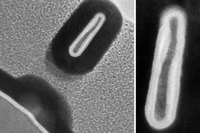
When etching away material, only 0.02nm of material was removed on each pass. "In each cycle, we can etch away just 2 percent of a nanometer of a material. That gives us super high accuracy and careful control of the process," says MIT graduate student Wenjie Lu.

During commercial manufacturing processes, atomic layer deposition (ALD) is already being used. Integration of the newer thermal atomic layer etching process can be done during the same phase as ALD, requiring only a "small redesign of the deposition tool to handle new gases to do deposition immediately after etching."

As an added benefit, materials are not exposed to ambient conditions as often, leaving less time and surface area for oxidation to occur. The end result is higher quality transistors with greater immunity to imperfections.

On average, the researchers' transistors were under 5nm wide and stood around 220nm tall. A 60 percent improvement in transconductance, the measure of energy it takes to convert voltage into current used for computation, was achieved compared to existing FinFET technologies.

Permalink to story.

 
All this transistor tech has one huge Achilles Hill - it is very susceptible to all kinds of magnetic interference, which limits its use for medical purposes, while at the same time it is the medical fields that seek most to adapt electronic solutions that fit minuscule profile.

That's why optical + vacuum tubes chip researches are way more fun.
 
Yeah but this gives us something to the Russians with a note to try to drill holes in it!
 
I'm really confused by this article.
"Repeating several hundred times allows a transistor to be built up layer by layer."
How is this mass manufacturing friendly? Seems like an extremely expensive process.

"On average, the researchers' transistors were under 5nm wide"
So not only it's not 2.5nm, but it's extremely variable in the outcome? Or have they only pushed to 2.5nm on select few transistors?

"When etching away material, only 0.02nm of material was removed on each pass"
Maybe I have flawed understanding, but isn't the radius of an atom is more like 0.2-0.5nm? How can you shave off 0.02nm of it?
 
"When etching away material, only 0.02nm of material was removed on each pass"
Maybe I have flawed understanding, but isn't the radius of an atom is more like 0.2-0.5nm? How can you shave off 0.02nm of it?

You should be confused, because we're being spun by the salesmen of this tech. The electron radius is 0.00000000244nm. The proton radius is 0.00000409nm. So that is effectively the radius of hydrogen, until the electron comes into play to expand it slightly. But even then, they are nowhere NEAR a nanometer apart, and the (corrected) Bohr radius is still far smaller than a nanometer.

Just as we've seen with graphene propaganda, they are TELLING us that they're working at the atomic level, when they are nowhere near it. They are still well, well above the molecular level and always will be, until they figure out how to ditch the electron and use photons exclusively. As it stands, they're just using photons to push electrons around, which is why these things are so inefficient to begin with and why our CPUs and GPUs get so hot. Every infrared photon emitted is wasted energy.
 
I'm really confused by this article.
"Repeating several hundred times allows a transistor to be built up layer by layer."
How is this mass manufacturing friendly? Seems like an extremely expensive process.

Current 12nm processes already go through hundred+ steps. The only way to cut down on the number of steps is by getting newer lithography machines. Those are coming in but they are extremely expensive.
 
You should be confused, because we're being spun by the salesmen of this tech. The electron radius is 0.00000000244nm. The proton radius is 0.00000409nm. So that is effectively the radius of hydrogen, until the electron comes into play to expand it slightly. But even then, they are nowhere NEAR a nanometer apart, and the (corrected) Bohr radius is still far smaller than a nanometer.

Just as we've seen with graphene propaganda, they are TELLING us that they're working at the atomic level, when they are nowhere near it. They are still well, well above the molecular level and always will be, until they figure out how to ditch the electron and use photons exclusively. As it stands, they're just using photons to push electrons around, which is why these things are so inefficient to begin with and why our CPUs and GPUs get so hot. Every infrared photon emitted is wasted energy.


Where do you get these numbers? First thing I get when I google is this:
"The electronic configuration of the silicon atom is: (Ne)(3s)2(3p)2, and the atomic radius is 0.132 nm. Silicon has the diamond cubic crystal structure with a lattice parameter of 0.543 nm. The nearest neighbor distance is 0.235 nm."

It's nowhere near 0.00000409nm.
He obviously used his Walmart ruler to measure those with that precision, what's the matter with you, don't you know a stranger on the internet is always right?
 
Back