First look: Intel's latest CPUs aren't headed to retail shelves or gaming rigs, but to the far edges of industrial computing. With the debut of its Bartlett Lake lineup, the company is doubling down on performance-focused silicon built for stability and predictability rather than raw frames per second.
The new family of chips, totaling 11 SKUs, expands Intel's embedded and edge portfolio. Each processor takes a uniform approach: an all-P-core design that discards the efficiency cores Intel has bundled with its consumer CPUs since 12th-gen Alder Lake. The move simplifies scheduling and reduces the overhead that can emerge from hybrid configurations.
Bartlett Lake is built on the Intel 7 process node, a refined 10nm-class design, and draws from the same Raptor Cove microarchitecture as the company's 14th-gen Raptor Lake chips. Instead of chasing consumer benchmarks, Intel tuned these CPUs for "deterministic" performance – the ability to guarantee consistent timing and predictable response rates.
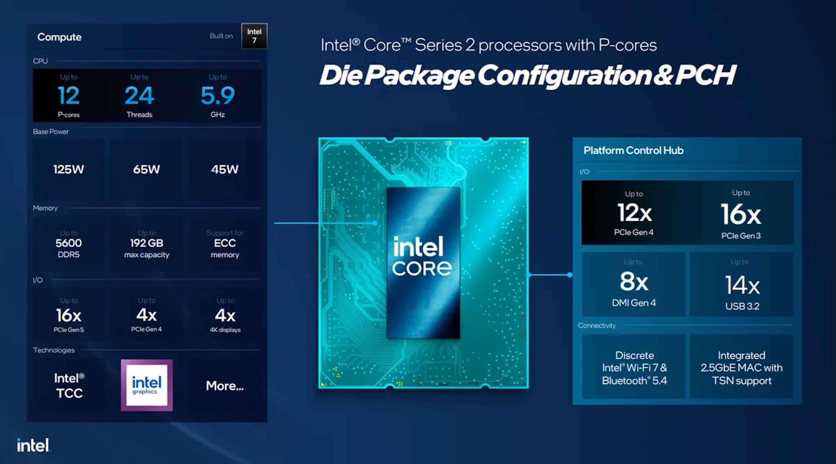
The series includes 12-, 10-, and 8-core models scaled across three thermal design points: 125W, 65W, and 45W. A lower-clocked 65W and 45W Core 5 variant trims an additional 200MHz from boost and base frequencies to match power-efficiency constraints.
Intel is backing the lineup with features tailored to embedded and industrial environments. Bartlett Lake offers Long-Term Servicing Channel support on Windows, ensuring extended system reliability in deployments that may remain operational for years.
The chips also support Time Coordinated Computing and Time-Sensitive Networking, which are capabilities vital for systems that rely on synchronized operations, such as factory robots, autonomous platforms, and 5G edge nodes.
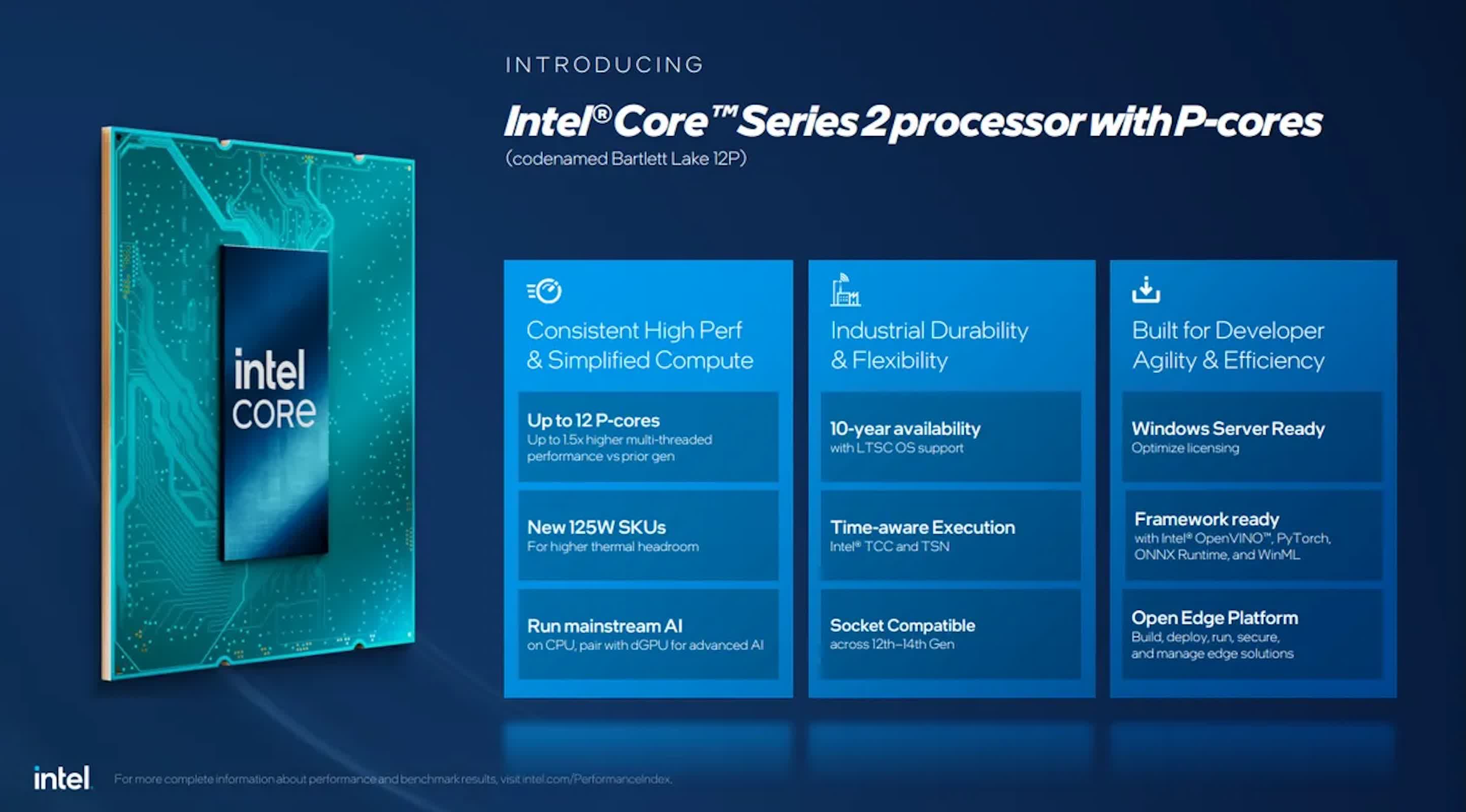
These choices reflect Intel's strategy to lean into deterministic rather than opportunistic computing. Eliminating hybrid scheduling reduces jitter in workloads that depend on precise task timing. For an industrial controller or a real-time analytics system, that can mean the difference between consistent output and unpredictable lag.
Connectivity mirrors Intel's mainstream platforms but is tuned for flexibility at the edge. Each Bartlett Lake CPU provides up to 16 PCIe 5.0 lanes and four PCIe 4.0 lanes directly from the processor. The accompanying platform controller hub extends that with 12 additional PCIe 4.0 lanes and 16 PCIe 3.0 lanes, plus eight lanes of the Direct Media Interface 4 (DMI 4), a high-bandwidth bridge first introduced with Intel's 600-series chipsets.
Memory support matches modern standards, topping out at 192GB of DDR5 at speeds up to 5,600MT/s with ECC support. For industrial developers and system integrators, this combination enables high data throughput and error correction without stepping up to entirely new platforms. Crucially, Bartlett Lake remains compatible with the existing LGA 1700 socket, maintaining continuity with 12th- through 14th-gen hardware ecosystems.
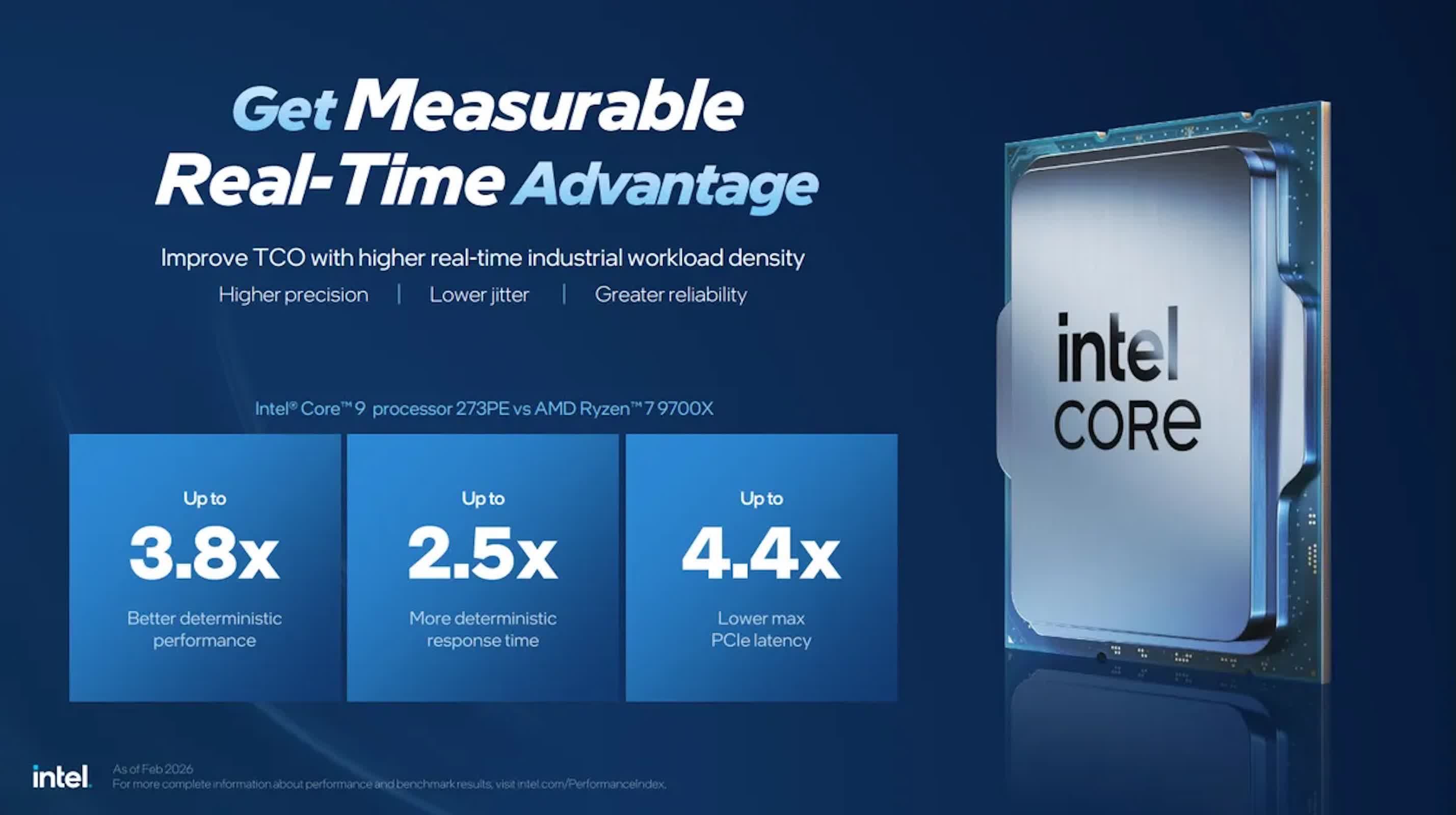
Intel's own performance comparisons center on reliability rather than benchmark scores. According to the company, the 12-core Core 9 273PE with a 65W TDP delivers up to 4.4 times lower maximum PCIe latency, a 2.5-times improvement in deterministic response, and up to 3.8 times better deterministic performance than AMD's embedded Ryzen 7 9700X. Intel has yet to release raw benchmark data or detailed methodology, and those metrics remain unverified outside the company's performance index.
For now, Intel has withheld both pricing and a defined release schedule, since these chips will ship exclusively through OEM and industrial channels rather than retail. Any appearance in consumer systems would likely arise only through gray-market resellers.
Alongside Bartlett Lake, Intel spotlighted performance gains from its Core Ultra Series 3 – previously known as Panther Lake – in edge and robotics contexts. The company compared its upcoming SoC to Nvidia's 64GB Jetson AGX Orin modules, claiming up to 1.7× faster image classification, 1.9× lower latency for large language models, and 4.5× higher throughput for vision-based action models.
Intel says these improvements could translate into significant total cost savings, citing potential reductions of more than $5,500 per system when replacing dual-accelerator setups with a single Panther Lake SoC.
Taken together, Bartlett Lake and the broader edge roadmap suggest Intel is optimizing its silicon portfolio for determinism and control rather than peak benchmark wins. The company's embedded strategy prioritizes maturity, compatibility, and long-term reliability – steady characteristics that stand in stark contrast to the volatility of the consumer CPU race.
Intel launches Bartlett Lake CPUs with all P-cores for embedded applications


